CXMT and YMTC factories are expanding, it will take at least another 1-2 years for them to fill the gap...I really hope that China increase their memory production capacity fast.
You are using an out of date browser. It may not display this or other websites correctly.
You should upgrade or use an alternative browser.
You should upgrade or use an alternative browser.
Chinese semiconductor thread II
- Thread starter vincent
- Start date
Heyan Technology proudly launches its 100th Jig Saw series (cutting and sorting integrated machine) product!
Today, representatives from the R&D, sales, production, and supply chain departments of Heyan Technology's Jig Saw series products gathered together to witness an exciting and glorious milestone in Heyan Technology's development history— the official shipment of the 100th Jig Saw series (cutting and sorting integrated machine) product!
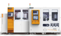
Looking back on the growth of the Jig Saw series products, from overcoming the challenges of the first unit to the mature and stable delivery of the hundredth, every step of growth embodies the wisdom of all colleagues, and every breakthrough is inseparable from the close collaboration of various teams. Zhang Mingming, Executive Vice President of the company, expressed his heartfelt gratitude to all the teams involved in the Jig Saw series project and affirmed the important significance of this product series to the company's strategic layout. Subsequently, Chen Qiang, General Manager of the JS Product Line, fondly recalled the arduous journey of the Jig Saw series from blueprint conception to mass production, and now to the delivery of the hundredth unit, highly praising the team's fighting spirit.
As the entire audience counted down in unison, "3-2-1!", the red silk covering the equipment was unveiled, officially revealing this device carrying special significance, ready to embark on a new journey to create value for customers. At that moment, applause and music intertwined, glory and dreams soared together!
The successful shipment of the 100th Jig Saw series (cutting and sorting integrated machine) is not the end, but a brand new beginning. It signifies that Heyan Technology's products and technologies have won deep market recognition, and it also instills in us the confidence and strength to move towards higher goals. All Heyan employees will take this opportunity to uphold our original aspirations, work together, and create greater value for customers with better products and services, contributing more "Heyan strength" to the progress of the industry!
The Institute of Microelectronics has made progress in the research of large-scale neural network attention accelerators.
The widespread application of large models based on Transformer neural networks (BERT, GPT, etc.) has enabled machines to possess understanding and expression capabilities closer to humans, demonstrating the enormous potential of artificial intelligence in improving productivity. The attention mechanism plays a crucial role in the computational energy consumption and latency of Transformers, making the design of energy-efficient and high-speed accelerators targeting this mechanism of significant research value. However, existing attention accelerator hardware architectures suffer from two main limitations: first, the commonly used systolic array architecture with fixed inputs, weights, and outputs cannot achieve a balance between data reuse, register usage, and utilization; second, the sequential computation of each layer leads to excessive SRAM access overhead for intermediate results. These limitations hinder further improvements in accelerator energy efficiency and speed.
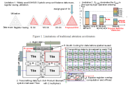
To address these challenges, a research team from the National Key Laboratory of Integrated Circuit Manufacturing Technology at the Institute of Microelectronics, Chinese Academy of Sciences, designed a high-energy-efficiency, high-utilization attention accelerator hardware architecture. This architecture employs a "Balanced Systolic Array" structure with a hybrid inner-outer product. Guided by data reuse theory, the team determined the optimal shape for the hybrid inner-outer product array, achieving a 40% improvement in energy efficiency and a 99.5% utilization rate compared to traditional systolic arrays. In terms of operation, the team proposed a "Multi-Row Interleaved" operation sequence, reducing SRAM power consumption by 31.7%. Based on these two technologies, the team's attention accelerator achieves a 39% improvement in energy efficiency and a 38% improvement in throughput × energy efficiency compared to existing work.
This research, titled " An Energy-Efficient High-Utilization Hardware Architecture for Attention Mechanism in Transformer using Balanced Systolic Array and Multi-Row Interleaved Operation Ordering, " was presented orally at the 62nd International Conference on Design Automation (DAC). Master's student Zhou Haiyang is the first author, and Assistant Researcher Hu Hongyang is the corresponding author.
Kostech: RF transceiver chip R&D project achieves phased results
Cosun Technology announced that its subsidiary, Shenzhen Gaoxinsi Technology Co., Ltd. (hereinafter referred to as "Gaoxinsi"), has completed the trial production and tape-out of its radio frequency transceiver chip, and has completed basic functional and performance testing. This marks a significant milestone in the R&D project. Gaoxinsi will continue to advance comprehensive testing of the chip's functions and performance.
According to available information, Costech was founded in 2004 and has been deeply involved in the field of military electronic information equipment. Its core products cover command and control information processing equipment and systems, software radar information processing equipment and systems, intelligent unmanned equipment and systems, etc.
Founded in 2015, High-Tech is a 94.6548% owned subsidiary of Kosun Technology, focusing on the integrated R&D and application of next-generation intelligent wireless baseband chips and wireless RF transceiver chips. Its mass-produced baseband chips are adaptable to various network configurations, meeting the diverse needs of handheld, mobile, and fixed devices.
Lianyong Microelectronics plans to invest 2.262 billion yuan to expand its production capacity of heavily doped large silicon wafers.
On the evening of November 17th, Lianyong Microelectronics announced that its controlling subsidiary, Jinruihong Microelectronics, signed an agreement with the Quzhou Intelligent Manufacturing New City Management Committee to construct a "1.8 million 12-inch heavily doped substrate wafer production project per year" within its existing factory buildings. The total investment for this project is approximately RMB 2.262 billion. The project construction period is approximately 60 months and will be carried out in phases, with an estimated annual investment of approximately RMB 350 million.
Data shows that Jinruihong Microelectronics focuses on the production of 12-inch heavily doped silicon wafers. Its 12-inch heavily doped epitaxial wafers meet the demands of high-end power devices, with applications in AI server uninterruptible power supplies, energy storage converters, charging piles, industrial electronics, servo drives, as well as consumer electronics, automotive electronics, home appliances, embedded systems, and industrial control, among other fields, indicating broad market demand. Jinruihong Microelectronics' existing heavily doped silicon wafer production capacity is ramping up rapidly and is currently nearing full capacity.
Lianyong Microelectronics stated that this project aims to meet the market demand for high-end power devices, especially the urgent need for thick-layer and buried-layer silicon epitaxial wafers with special specifications, such as those heavily doped with arsenic and phosphorus. Upon completion, the project will add an annual production capacity of 1.8 million 12-inch heavily doped substrate wafers, further enhancing the company's production capacity of heavily doped silicon wafers, optimizing its product structure, increasing product diversity, and further meeting the demands of the integrated circuit market, thereby improving the company's overall competitiveness.
Bio-Chem's subsidiary is leading the research and development of next-generation dry etching equipment, with a planned investment of 218.6 million yuan of its own funds.
through its subsidiary Xinhuilian (Foshan) Semiconductor Technology Co., Ltd. (hereinafter referred to as "Foshan Xinhuilian"), plans to take the lead in signing a cooperative R&D project contract with well-known domestic universities and research institutions to develop next-generation dry etching equipment. Foshan Xinhuilian plans to invest RMB 218.6 million (approximately RMB 218.6 million) of its own funds in this project.
The announcement indicates that the collaborative R&D project has been approved by the 18th meeting of the 5th Board of Directors of Bio-Tech Chemicals and does not require submission to the shareholders' meeting for review. It does not constitute a related-party transaction or a major asset restructuring. Foshan Xinhuilian will lead the project, with its director and co-general manager Liu Hongjun serving as the project leader. The company will form a consortium with renowned domestic universities and research institutions to jointly promote the R&D and industrialization of next-generation dry etching equipment.
It is understood that dry etching equipment is one of the key pieces of equipment in the semiconductor manufacturing field, and the development of high-generation equipment is of great significance for enhancing the self-reliance and controllability of China's semiconductor industry chain. Bio-Chem stated that this collaboration aims to leverage the company's R&D team's technological expertise in etching equipment, and through deep industry-academia-research collaboration, accelerate the technological breakthroughs and industrialization of domestically produced high-generation etching equipment.
Foshan Xinhuilian plans to invest 218.6 million yuan, all from its own funds, specifically for equipment procurement, material research and development, testing services, and other related expenses during the project's R&D process. According to the contract, the project management unit (Party A) will allocate a portion of the R&D funds annually. Foshan Xinhuilian is required to establish a dedicated account for separate accounting of these funds, ensuring that they are used for their designated purpose and accepting supervision and inspection from Party A and relevant institutions.
The core objective of the project is to overcome key technological bottlenecks in next-generation dry etching equipment and promote the substitution of domestically produced equipment in the semiconductor manufacturing field. Bio-Chem points out that this project closely aligns with the company's semiconductor business development strategy, providing technical support for the company's continued output of diversified products and services, while deepening collaborative innovation with universities and research institutions to enhance the efficiency of the company's overall R&D system.
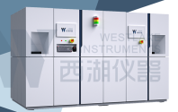
Westlake Instruments' diamond laser lift-off equipment was launched and shipped immediately, marking a step towards industrialization.
Westlake Instruments showcased its new "Diamond Laser Lifting Equipment" at the "2025 Optoelectronic Technology and Industry Development Forum" hosted by the Institute of Optoelectronics, Westlake University. During the event, the company officially launched the equipment and announced that the first unit had been prepared and would be delivered to the customer within two days after the forum, achieving "release and shipment immediately".
This progress not only signifies that the product's technological maturity has been validated by the market, but also marks a further acceleration in the industrialization of diamond equipment.
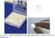
Leveraging groundbreaking laser-guided lithography technology, this equipment can control material loss to approximately 100 μm when processing 1-inch diamond substrates, reducing processing time from several hours using traditional methods to less than 20 minutes (optimal data). While ensuring high yield and consistency, it significantly reduces processing costs, providing an equipment foundation for the large-scale production of large-size diamond substrates.
Lion semiconductor announces plan for a new 12-inch wafer project with 2.262B RMB investment. Will produce 1.8m heavily doped wafers per year. Work to start in December 31st of this year and full construction period is 5 years. I'm assuming that it will start production before that.
Seems like this heavily doped substrate is need in AI data center's uninterruptible power supplies, energy storage converters, charging piles, industrial electronics, and automotive electronics.
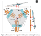
Wrench Model with Rotation Angles for Magnetically Levitated Actuators
Abstract
Magnetic levitation actuators (MLAs) are frequently employed in photolithography, precise positioning and transportation. The actuator, which consists of racetrack coils and one-dimensional 3 Halbach arrays, has the capacity to calculate the wrench model in real time. However, the high computational demands of the high-dimensional wrench model will result in a prolonged control cycle. Based on a levitation plane composed of three groups of magnetic levitation actuators, this paper proposes a wrench model considering six dimensions to calculate the output current required by the actuator in real time. This method simplifies the expression form of the formula and directly calculates the expression of the current conversion matrix, thereby enabling the system’s computing speed to reach 3 KHz. The system’s step response and trajectory-tracking performance were simulated and compared under the models with and without angular consideration. It has been demonstrated that when rotation angles are incorporated into the magnetic levitation plane, the wrench model considering angles achieves better performance than the wrench model without rotation angles.
Anlogic/安路科技 has Phoenix series FPGA using 28nm process in production. It says localization of FPGA in China has already reached 30% as of 2025. It also has FPSoC (integrates processor w/ FPGA on same chip) for industrial control & video processing.
Also, looks like FPGA demand is really going up due to data center and AI demand.
