I mean. We’ll see. The Kirin 930 will be the barometer for where advanced node domestic fabbing currently is. Tbh I’m not expecting to be blown away.
Mate 80 pre-order should be starting any moment and it will have launch event on 25th. Should come with Kirin 9030 and 20GB DRAM. Expect some pretty huge upgrade in Kirin chip, process and the entire supply chain, including 3D facial recognition tech.
You are using an out of date browser. It may not display this or other websites correctly.
You should upgrade or use an alternative browser.
You should upgrade or use an alternative browser.
Chinese semiconductor thread II
- Thread starter vincent
- Start date
antiterror13
Brigadier
I mean. We’ll see. The Kirin 930 will be the barometer for where advanced node domestic fabbing currently is. Tbh I’m not expecting to be blown away.
Will it still be 7nm? I am hopeful 5nm
5nm or 6nmWill it still be 7nm? I am hopeful 5nm
it's expected to be somewhere like the original Samsung 5nm, which is TSMC N6, in transistor density.5nm or 6nm
Axera, which produces AI chips for auto and edge scenarios, already have M55H in production. Will now launch M57 chip for next generation ADAS. Works with partner on AI 4D MMW radar solution.
It has already delivered almost 1 million chips to auto industry. Mostly for lower end image processing type of chips.
fyi, I've personally tested out running boards with Axera AI chips and they have some of the best software support for a startup. Very impressive for a new company.
Will it still be finfet with comventional materials and interconnects?it's expected to be somewhere like the original Samsung 5nm, which is TSMC N6, in transistor density.
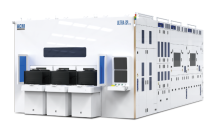
Shengmei Shanghai delivered its first horizontal panel electroplating equipment, effectively responding to the market demand for advanced packaging!
Shengmei Shanghai delivers its first horizontal panel electroplating equipment, Ultra ECP ap-p
The Ultra ECP ap-p is the first commercially available panel-grade copper plating system for the large-panel market, supporting plating steps in pillar, bump, and redistribution layer (RDL) processes. This system achieves panel processing performance comparable to traditional circular wafer processes, enabling manufacturers to more efficiently meet demanding device requirements.
ACM Research (Shanghai) Co., Ltd. ("ACM Research Shanghai") (Science and Technology Innovation Board stock code: 688082), a leading supplier of wafer process solutions for semiconductor front-end and advanced wafer-level packaging applications, today announced the successful delivery of its first panel-level advanced packaging electroplating equipment, Ultra ECP ap-p, to a leading panel manufacturing customer. This achievement not only demonstrates ACM Research Shanghai's significant progress in the field of panel-level advanced packaging electroplating technology, but also reflects the growing market demand for scalable, low-cost advanced packaging solutions.
Wang Jian, General Manager of Shengmei Shanghai, stated:
We are delighted to have successfully delivered the Ultra ECP ap-p order. This milestone underscores our ability, through differentiated innovation, to deliver high-performance panel plating solutions that help customers accelerate their fan-out panel-level packaging technology roadmaps, while solidifying our important position in the advanced packaging ecosystem. As market demand for next-generation devices grows, panel-level packaging offers the scalability, capacity, and cost advantages required for mass production, enabling a seamless transition from 300mm wafer packaging to panel-level packaging.

Key features of the product
This system employs horizontal electroplating technology protected by an ACM patent application and supports electroplating processes for multiple materials, including copper, nickel, tin-silver, and gold. The copper plating chamber is equipped with high-speed plating blades specifically designed for high-protrusion applications, enabling protrusion heights exceeding 300 micrometers. The Ultra ECP ap-p device utilizes a four-sided sealed dry contact chuck for enhanced reliability, features an in-chamber cleaning function to minimize chemical cross-contamination between different plating chambers, and employs a horizontal plating design—achieving superior film thickness uniformity through synchronously rotating chucks and a rotating rectangular electric field.
Projects such as the Microenvironment Control Semiconductor Equipment Microenvironment Control R&D Headquarters Base were signed and settled in Wuhan Optics Valley.
On November 15th, the 17th Huazhong University of Science and Technology (HUST) Entrepreneurs (Wuhan) Conference was held in Optics Valley, with over 1,500 HUST alumni, faculty, and student representatives from across the country in attendance. At the conference, 36 projects invested in or collaborated on by HUST alumni-owned companies were signed, totaling 15 billion yuan. Eight of these projects, with investments exceeding 8 billion yuan, were located in Optics Valley.
It is understood that the projects signed and settled in Optics Valley this time include Huayun Smart National Headquarters, Huawico Flexible Intelligent Sensing R&D and Pilot Production Base , and Microenvironment Control Semiconductor Equipment Microenvironment Control R&D Headquarters Base , etc., mainly targeting the fields of artificial intelligence, integrated circuits, etc., to develop the next generation of information technology of "optical chip screen terminal network".
Li Xiaoping, founder of Wuhan Microenvironmental Control Technology Co., Ltd. and professor at Huazhong University of Science and Technology, said: "As early as 20 years ago, our team began to develop microenvironmental control technology for high-end integrated circuit equipment. In 2021, based on the solid integrated circuit industry foundation of Optics Valley, we established a company locally to promote the transformation of our achievements, and business orders have steadily increased. After the R&D headquarters base is completed and put into use next year, the company is expected to achieve annual sales of over 100 million yuan."
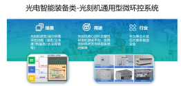
Wuhan Micro-Environmental Control Technology Co., Ltd. completed a Pre-A round of financing worth tens of millions of yuan in September this year. This is the company's second round of financing after its angel round, and the funds raised will be mainly used for new technology research and development and product capacity expansion. The company has successfully launched the first electromagnetic shielding micro-environmental control system in China specifically designed for electron beam lithography machines, and has also developed a complete micro-environmental control system for a certain type of domestic front-end lithography machine. For top-tier equipment and instruments such as lithography machines, coating and developing machines, metrology systems, bonding machines, and optical inspection machines, the company can provide complete sets of micro-environmental control systems and a series of supporting products, achieving temperature stability of ±5mK, liquid temperature and solid temperature stability of ±1mK, humidity stability of ±0.4%RH, air pressure stability of ±1Pa, electromagnetic shielding magnetic field fluctuation of 30nT, and cleanliness of ISO Class 1.
Optoelectronic Intelligent Equipment Category - General-purpose Micro-environmental Control System for Lithography Machines

