Chinese semiconductor thread II

huemens

Junior Member
Registered Member
BEUV(Beyond EUV Lithography)

View attachment 161810

Some Russian researchers recently proposed a plan for an 11.2nm light source.
Please, Log in or Register to view URLs content!

The Institute of Microstructure Physics of the Russian Academy of Sciences (via Dmitrii Kuznetsov) has laid out a long-term roadmap for domestic extreme ultraviolet (EUV) lithography tools operating at a wavelength of 11.2 nm, extending the information the organization shared last December.
The very first thing that strikes the eye is that the proposed EUV* systems avoid replicating the architecture of ASML's tools. Instead, the plan is to use an entirely different set of technologies: hybrid solid-state lasers, xenon plasma-based light sources, and mirrors made from ruthenium and beryllium (Ru/Be) that reflect light at a 11.2nm wavelength. The choice of xenon instead of tin droplets in ASML's EUV tools eliminates debris that harms photomasks, which dramatically reduces maintenance. Meanwhile, when compared to ASML's DUV tools, the lower complexity is meant to avoid high-pressure immersion fluids and multi-patterning steps for advanced nodes.
 

tokenanalyst

Lieutenant General
Registered Member

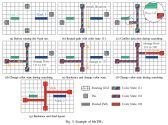
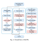
Mr.TPL: A Method for Multi-Pin Net Router in Triple Patterning Lithography.​


University of Science and Technology Beijing.
Tsinghua University
Empyrean Technology Co., Ltd., Beijing, China


Abstract—Triple patterning lithography (TPL) has been recognized as one of the most promising solutions to print critical features in advanced technology nodes. A critical challenge within TPL is the effective assignment of the layout to masks. Recently, various layout decomposition methods and TPL-aware routing methods have been proposed to consider TPL. However, these methods typically result in numerous conflicts and stitches, and are mainly designed for 2-pin nets. This paper proposes a multipin net routing method in triple patterning lithography, called Mr.TPL. Experimental results demonstrate that Mr.TPL reduces color conflicts by 81.17%, decreases stitches by 76.89%, and achieves up to 5.4× speed improvement compared to the state-of the-art TPL-aware routing method.​

1759171542967.png1759171595454.png

Please, Log in or Register to view URLs content!
 

tokenanalyst

Lieutenant General
Registered Member

Arctic Xiongxin GPU chip lights up.​


Arctic Xiongxin has successfully powered up its QM935-G1 IVI chiplet, a high-performance component designed for intelligent vehicle cockpits. Featuring a 1.3TFLOPS GPU and 51.2GB/s memory bandwidth, it supports advanced multimedia functions (like HiFi5 and UFS) and enables secure isolation between instrument clusters and entertainment systems.​

1759172987855.png

To meet the growing demand from AI-driven smart cockpit and autonomous driving applications, Arctic Xiongxin leverages chiplet technology to offer modular, scalable solutions:

The QM935-C08 combines one QM935-G1 GPU chiplet with HUB and Ursa Major AI chiplets, delivering up to 128GB/s memory bandwidth, ideal for large-scale AI operating systems (AIOS) and integrated cockpit platforms.
The QM935-A04 four-core module delivers 800TOPS computing power, enabling distributed AI processing for next-generation intelligent driving (VLA).
The QM935-G1 can act as a co-processor to enhance GPU rendering, addressing limitations in current cockpit chips.
Using its proprietary PBLink interconnect, the chip supports flexible memory expansion, enabling smooth multi-screen interaction, ultra-high-resolution displays, and real-time 3D rendering—ideal for AAA games, digital twins, and high-precision maps. This also allows for fast, offline AI assistant functionality with strong reasoning and multi-turn conversation capabilities.

With advancements in large model deployment, Arctic Xiongxin is positioning itself as an AI infrastructure provider for automotive applications, focusing on chiplet-based design and near-memory computing to support edge AI, vehicle-side intelligence, and future autonomous driving. The company aims to deliver cost-effective, high-performance "one-board" solutions that meet evolving demands in smart vehicles.​

Please, Log in or Register to view URLs content!
 

tokenanalyst

Lieutenant General
Registered Member

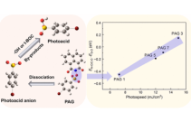
Mechanistic Insights into Acid Generation from Nonionic Photoacid Generators for Extreme Ultraviolet and Electron Beam Lithography.​

Abstract​

Nonionic photoacid generators (PAGs) have emerged as key components in advanced extreme ultraviolet (EUV) and electron beam (EB) photoresists, offering advantages such as low dark loss, reduced outgassing, and suppressed phase separation. However, the lack of molecular-level understanding of their acid generation mechanisms hinders rational design and leads to reliance on trial-and-error synthesis. In this study, we perform a comprehensive density functional theory (DFT) investigation on 22 representative nonionic PAGs to elucidate their postexposure reaction pathways, encompassing bond dissociation, byproduct formation, and proton transfer mechanisms. Our findings reveal four distinct electron-triggered dissociation modes, including productive N–O/C–O bond cleavage and competing, nonproductive S–O bond cleavage. We identify the relative energy barrier between productive and unproductive pathways as a critical descriptor for photoacid generation efficiency and, by extension, photoresist sensitivity. Moreover, we demonstrate that molecular conformation (bent vs extended) and electron-withdrawing or electron-donating substituents profoundly impact the selectivity of bond dissociation. Importantly, this study also clarifies the roles of various proton sources (phenolic −OH+, t-BOC+ protecting groups, and intermediates during byproduct formation) in facilitating acid formation. Our analysis quantifies the energy barriers associated with each route, highlighting structure-dependent modulation of acid generation efficiency. These insights collectively establish a structure–mechanism–function relationship for nonionic PAGs and offer a predictive framework for designing next-generation high-sensitivity PAGs tailored for advanced lithographic applications.

1759173498728.png

Please, Log in or Register to view URLs content!
 

tokenanalyst

Lieutenant General
Registered Member

300,000 tons of high-purity quartz sand and 10,000 quartz crucibles project will be launched in Shandong​


Recently, the People's Government of Shanting District, Zaozhuang City, issued a public announcement on the acceptance of environmental impact assessment documents for Shandong Jingbo Energy Technology Co., Ltd.'s high-purity quartz sand and quartz crucible production project.
Shandong Jingbo Energy Technology Co., Ltd. invested 120 million yuan to purchase ball mills , drum screens, magnetic separators, pickling tanks, steam boilers, dryers , color sorters and other equipment to build a high-purity quartz sand and quartz crucible production project.
The project uses quartz sand, hydrochloric acid and other raw materials, and manufactures high-purity quartz sand through processes such as feeding, screening, ball milling, screening, desludging, magnetic separation, separation, pickling, deacidification, drying, color sorting, and fine grinding; uses high-purity quartz sand, barium hydroxide and other raw materials, and manufactures quartz crucibles through processes such as arc melting, demolding, sandblasting, cutting, pickling, water washing, drying, and barium coating. After completion, the project will achieve an annual output of 300,000 tons of high-purity quartz sand and 10,000 quartz crucibles.

Please, Log in or Register to view URLs content!
 

tokenanalyst

Lieutenant General
Registered Member

Shengmei Shanghai disclosed that the total amount of backlog orders was 9.072 billion yuan, an increase of 34.10% year-on-year​

hengmei Shanghai announced that as of September 29, 2025, the company's total order backlog amounted to 9.072 billion yuan, a year-on-year increase of 34.10%. These orders include equipment orders that have been delivered to customers but for which revenue has not yet been recognized, as well as equipment orders to be delivered in the future.

Founded in 2005, Shengmei Shanghai is a semiconductor equipment manufacturer focusing on advanced integrated circuit manufacturing and advanced wafer-level packaging manufacturing industries. It is mainly engaged in the research and development, manufacturing and sales of single-wafer and tank wet cleaning equipment, electroplating equipment, stress-free polishing equipment, vertical furnace tube equipment, front-end coating and development equipment, and plasma-enhanced chemical vapor deposition equipment.

Please, Log in or Register to view URLs content!
 

tokenanalyst

Lieutenant General
Registered Member

Crownstone Technology plans to raise 700 million yuan to increase its investment in localizing high-end mask plates.​


Driven by the wave of domestic semiconductor substitution Guanshi Technology disclosed its plan to issue shares to specific investors in 2025. The company plans to issue no more than 22.0405 million shares to no more than 35 qualified investors through a "competitive bidding + cash" method, raising no more than 700 million yuan.

The raised funds will mainly be used for the "Photomask Manufacturing Project" in Ningbo Qianwan New Area, of which 530 million yuan will be invested in 28nm and below process mask production lines, and 170 million yuan will be used to supplement working capital and alleviate operating capital pressure.

Reticle plates, a key material for semiconductors and new display devices, serve as pattern transfer masters, transferring circuit patterns onto substrates or wafers through exposure for mass production. The global semiconductor mask market is projected to reach US$8.94 billion in 2025, with the domestic market estimated at approximately RMB 18.7 billion. This market is expected to continue to grow. However, my country lags behind in the mask market overall, with the global third-party semiconductor mask market dominated by international giants such as Phoenix (US), Toppan Printing (Japan), and Dai Nippon Printing (Japan). my country's photomask industry developed late, relying on imports for key raw materials and equipment. The mid- to high-end market is still dominated by foreign manufacturers, resulting in a low domestic content rate of approximately 10% overall and only 3% for high-end photomasks. This leaves significant room for domestic substitution. For this reason, mask plates have been designated as a key support sector, enjoying preferential tax policies. Currently, domestic substitution of semiconductor photomasks has entered a comprehensive phase.

The plan states that this private placement has three main objectives. First, it aims to improve equipment support capabilities and enhance the competitiveness of existing businesses. The company has already launched new 55nm products and successfully completed the 40nm production line. The raised funds will increase investment in backup equipment and testing equipment for key process links. Second, it aims to introduce mid- to high-end process equipment to promote iterative upgrades of mask plates. The 28nm mask production line is a key bridge and core battlefield. The raised funds will help the company achieve high-end breakthroughs and large-scale development. Third, it aims to strengthen the company's capital strength and enhance its risk resilience. As the business scale expands, the company's notes and accounts receivable and short-term loans will increase. Once the raised funds are in place, net assets will increase, the debt-to-asset ratio will decrease, and financial expenses will be saved.

The project implementation is feasible. The company has relevant management experience and good cooperation with many leading display panel manufacturers. It can apply its existing business experience to the field of semiconductor masks. The project team has rich operational experience. It is led by a senior expert and a team of about 40 people with practical experience in all aspects. The company planned the project in 2021 and established a subsidiary to implement it in 2023. It has completed many important node goals ahead of schedule and built a complete manufacturing system. The project has been partially completed and put into production, the basic construction of the factory building has been completed, and the main production equipment has been installed and debugged. As of the end of August 2025, the cumulative revenue has reached approximately RMB 10.1873 million. Revenue is expected to increase after the product verification cycle is completed.

Please, Log in or Register to view URLs content!
 

tokenanalyst

Lieutenant General
Registered Member

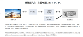
Zhixin Microelectronics' Nantong module plant is completed, accelerating its silicon carbide layout​


The Zhixinwei (Nantong) module factory officially started construction. The Zhixinwei (Nantong) project is jointly supported by the Shenzhen Major Industrial Investment Group and the Nantong Chongchuan Xinchuang Industrial Investment Fund. The Nantong module factory plans to build two flexible production lines:

Glue filling module line: compatible with EASY, 34MM and other specifications of products, with an annual production capacity of 200,000 units;

Plastic-encapsulated module line: supports SOT-227, IPM and other package types, with an annual production capacity of 1 million units.

In order to strengthen the layout of the automotive-grade market, the factory will also set up dedicated automotive-scale block production lines such as TPAK and DCM to further enhance the coverage of high-reliability scenarios such as new energy vehicles, photovoltaics, and power grids.

1759248602486.png

Please, Log in or Register to view URLs content!
 

tokenanalyst

Lieutenant General
Registered Member

ProLiant's FS800 device parameter analyzer won the bid for Nanjing University's semiconductor electronics measurement project​


ProLiant's FS800 device parameter analyzer, featuring independent intellectual property rights, has been selected as the winning solution for Nanjing University’s semiconductor electronics measurement project, marking a major milestone in advanced scientific research support. The FS800 is a high-precision, integrated electrical testing platform designed to meet the rigorous demands of cutting-edge semiconductor development—particularly in memristors and neuromorphic devices. It enables comprehensive characterization of device physical properties across material research, fabrication, and system-level application development by delivering accurate, real-time data essential for breakthroughs in post-Moore era technologies.​

1759249356131.png

Built on ProLiant’s proprietary modular hybrid architecture with a high-speed data bus, the FS800 combines current-voltage (IV), capacitance-voltage (CV), fast waveform generation, and time-domain signal acquisition into one flexible benchtop system. Its core component, the in-house developed FS810 SMU module, offers fA-level current resolution, wide measurement ranges, and exceptional accuracy—critical for detecting subtle electrical behaviors in 2D materials and memristors. With a sampling rate up to 100 MS/s and pulse width down to 130 ns, the system captures dynamic resistive switching and synaptic conductivity changes under stimulus, enabling precise analysis of learning behaviors and device reliability in brain-inspired architectures.

Equipped with LabExpress software, the FS800 provides an intuitive interface and pre-built test algorithms for static/dynamic verification and reliability evaluation, allowing researchers to conduct complex experiments without programming. The platform supports customizable scripting, batch testing, real-time visualization, statistical analysis, and seamless data export—significantly streamlining research workflows from material discovery to device deployment. This successful bid underscores ProLiant’s technological leadership in semiconductor measurement solutions and reflects its commitment to empowering scientific innovation through intelligent, scalable, and high-precision instrumentation that accelerates R&D cycles across next-generation electronic systems.​

Please, Log in or Register to view URLs content!
 
Top