Yangtze Memory Breaks Ground on Phase-III Project, Aims to Capture 15% Global NAND Market Share with Pricing Power in Sight
China’s domestic memory chip industry has achieved a significant milestone. According to Tianyancha APP and official corporate information, Yangtze Memory Phase-III (Wuhan) Integrated Circuit Co., Ltd. was officially established on September 5, 2025, with a registered capital of RMB 20.72 billion. It is owned 50.19% by its parent company, Yangtze Memory Technologies Co., Ltd. (YMTC), and 49.81% by Hubei Changsheng Phase-III Investment Development Co., Ltd., an entity backed by Hubei state-owned capital. The legal representative is Chen Nanxiang, Chairman of Yangtze Memory.
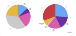
This move is widely regarded as a key signal of YMTC's Phase-III capacity expansion. Public data indicates that YMTC's current monthly production capacity is close to 130,000 wafers, accounting for approximately 8% of the global 3D NAND market. The company plans to increase its monthly capacity to 150,000 wafers by 2025 and aims to capture 15% of the global NAND flash supply by the end of 2026. According to earlier environmental impact assessment information, its overall planned capacity is 300,000 wafers per month, with each phase targeting 100,000 wafers. The establishment of this Phase-III entity signifies that YMTC is steadily advancing toward doubling its total production capacity, further addressing the urgent domestic demand for independently controllable storage products.
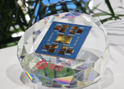
Since its inception in 2016, YMTC has consistently focused on the research, development, and industrialization of 3D NAND flash technology. Even after being added to the U.S. Entity List in late 2022 and facing restrictions on equipment imports, the company has persisted in pursuing independent innovation. Its self-developed Xtacking® architecture has been iterated to version 4.0, successfully achieving mass production of 3D NAND Flash with over 232 layers. Currently, YMTC has begun shipping 232-layer TLC chips (X4-9070), which utilize a double-stacked structure to achieve a total of 294 layers and an interface speed of 3600 MT/s. The product performance has reached international first-tier standards.
From a market perspective, global NAND flash demand is gradually recovering, with some international brands already initiating price hikes. Additionally, China accounts for over 30% of global NAND market sales, providing solid market momentum and strategic significance for YMTC’s capacity expansion. If the monthly production capacity reaches 200,000 wafers, YMTC will possess the pricing power to influence global NAND flash market trends.
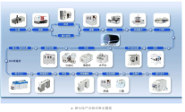
It is worth noting that while advancing capacity expansion, YMTC is accelerating the localization of its supply chain. According to reports, the company plans to initiate trial production on its first fully domestically equipped production line in the second half of 2025. This move aims to reduce reliance on foreign equipment and is a critical step in responding to U.S. export controls. Currently, the localization rate of YMTC’s equipment has reached 45%, significantly higher than that of other major domestic wafer fabs.

