Chinese semiconductor thread II

tokenanalyst

Lieutenant General
Registered Member

Zhaoxin KH-50000 processor makes its physical debut, and the domestically produced computing power base has reached the same level as international flagships​


The 2025 China International Communications Exhibition (PT Exhibition) opened grandly in Beijing. Hailed as a barometer of communications industry development and a bellwether of technological evolution, the PT Exhibition serves as a vital window into the latest developments in the information and communications industry.

At this year's exhibition, Zhaoxin's new Kaisheng KH-50000 server processor made its physical debut. It uses an LGA package with dimensions of 72 x 76mm, a step up from the previous-generation KH-40000 processor (56.5 x 77.5mm).
806991523783.3628.jpg

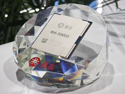
The Kaisheng KH-50000 utilizes a chiplet architecture, significantly improving computing density. It supports up to 96 CPU cores per socket and features a 384MB cache. This represents a 200% increase in core count compared to the previous-generation KH-40000 (32 cores), bringing its single-socket performance density close to that of the AMD EPYC 9755 (128 cores/512MB cache) . The CPU can reach a clock speed of 2.2 to 3.0GHz.

In addition, Kaisheng KH-50000 has also fully upgraded its IO interface, supporting up to 12 channels of DDR5 ECC memory, 128 channels of PCIe 5.0/ZPI/CXL and 16 channels of PCle 4.0/SATA/USB and other mainstream IO, supporting dual-channel and quad-channel interconnection , achieving greater data bandwidth, lower latency and power consumption.

Kaisheng KH-50000 processor can be used for computing platforms such as workstations, general-purpose servers, high-density AI servers, and high-density storage servers, and can provide a stronger hardware foundation for complex computing scenarios.

Please, Log in or Register to view URLs content!
 

tokenanalyst

Lieutenant General
Registered Member

North China Huachuang: Accelerating new product R&D and continuously strengthening the advantages of the integrated platform.​


The company successfully completed the acquisition of Xinyuan Micro, adding core photolithography equipment such as coating and developing equipment to its portfolio, further improving its integrated circuit equipment product line layout and process coverage. By integrating resources in marketing, technology, and supply chains, the company has effectively enhanced its overall competitiveness in the integrated circuit equipment market, further consolidating its platform advantages.

R&D and innovation have yielded fruitful results, and a new product pipeline is poised for future growth. The company is driving innovation with intensive R&D investment, reaching 2.9 billion yuan in the first half of the year, a 30% year-on-year increase. In March of this year, the company officially entered the ion implantation equipment market and subsequently launched a series of new products, including electroplating equipment. Among them, the SICRIUS PY302 series 12-inch advanced low-pressure chemical vapor silicon deposition vertical furnace has been validated by multiple wafer fabs and has entered mass production.

Please, Log in or Register to view URLs content!
 

tokenanalyst

Lieutenant General
Registered Member

Precision Microenvironment-Driven Isothermal Annealing for the Self-Assembly of Perpendicular Block Copolymers in High-Resolution Lithography Applications​

Abstract​

Block copolymer (BCP) nanolithography offers potential beyond traditional photolithographic limits, yet reliably producing low-defect, perpendicular domains remains challenging. We introduce a microenvironment-driven isothermal annealing method for directed self-assembly (DSA) of BCP thin films. By annealing films at stable temperature in a quasi-sealed, inert-gas chamber, our approach promotes highly uniform perpendicular lamellar nanopatterns over large areas, effectively mitigating environmental fluctuations and emulating solvent-vapor annealing without solvent exposure. Resulting BCP structures demonstrate enhanced spatial coherence and notably low defect density. Furthermore, we successfully transfer these nanopatterns into precise metal nano-line arrays, confirming the method’s capability for high-fidelity pattern replication. This scalable, solvent-free technique provides a robust, reliable route for high-resolution nanopatterning in advanced semiconductor manufacturing.

Please, Log in or Register to view URLs content!
 

tokenanalyst

Lieutenant General
Registered Member

Highly Selective Isotropic Etching of Si to SiGe Using CF4/O2/N2 Plasma for Advanced GAA Nanosheet Transistor.​

Abstract​

The paradigm shift from FinFET to gate-all-around nanosheet (GAA-NS) transistor architectures necessitates fundamental innovations in channel material engineering. This work addresses the critical challenge of pFET performance degradation in GAA-NS technologies through the development of an advanced selective etching process for strain-engineered SiGe channel formation. We present a systematic investigation of Si selective etching using CF4/O2/N2 gas mixture in a remote plasma source reactor. It is demonstrated that the addition of N2 to CF4/O2 plasmas significantly improves the selectivity of Si to SiGe (up to 58), by promoting NO* radical-induced passivation layer disruption on Si surfaces. Furthermore, an increase in the F:O ratio has been shown to mitigate stress-induced lateral micro-trenching (“Si-tip”), achieving near-zero tip length at high CF4 flow (500 sccm) while retaining selectivity (>40). Transmission electron microscopy and energy-dispersive X-ray spectroscopy confirm the complete removal of the Si sacrificial layer with minimal SiGe channel loss, validating the process for high-performance SiGe GAA-NS FET integration. These findings provide critical insights into strain-engineered SiGe channel fabrication, enabling balanced NFET/PFET performance in next-generation semiconductor technologies.​

1758851376854.png1758851410112.png

Please, Log in or Register to view URLs content!
 

tokenanalyst

Lieutenant General
Registered Member

Lingguang Infrared received tens of millions of yuan in A++ round financing, focusing on the analysis of chip electrical performance degradation.​

Anhui Lingguang Infrared Technology Co., Ltd. (Lingguang Infrared), a company specializing in chip performance degradation analysis solutions, recently completed a multi-million RMB Series A++ funding round led by IDG Capital and Qigao Capital.

According to information, Lingguang Infrared, founded in December 2021, specializes in the localization of high-end laboratory testing instruments to address pressing technical bottlenecks in high-precision equipment. The company's core products include phase-locked infrared thermal imagers, low-light-level microscopes, and laser-induced positioning systems. Their applications include, but are not limited to, chip failure analysis, electronic device thermal analysis, medical near-infrared imaging, material thermal conductivity testing, and bonding testing. The company's current products are primarily used for chip electrical failure analysis.

Lingguang Infrared is currently the only company in China that has successfully developed a complete set of semiconductor electrical failure analysis equipment that rivals imported equipment. Lingguang has also successfully transferred its underlying technology to applications in thermal management, material testing, and in vivo imaging

1758851856237.png1758851873863.png
1758851901511.png

Please, Log in or Register to view URLs content!
 

tokenanalyst

Lieutenant General
Registered Member

Integrated Circuit Intelligent Optimization Design Method


The team from the School of Integrated Circuits and Micro-Nanoelectronics Innovation has established artificial intelligence-based integrated circuit automatic optimization methods, machine learning-based integrated circuit statistical analysis methods, deep learning-based manufacturability design methods, and circuit comprehensive optimization, focusing on major demands such as domestic high-performance processor design and analog integrated circuit chip design. This provides a new theoretical framework and domestic tool support for artificial intelligence design EDA of analog integrated circuits and digital integrated circuits .

Analog integrated circuit design has long been a recognized challenge in the industry. Zeng Xuan's team innovatively proposed a method based on subspace theory and trust-region derivative-free optimization. This method uses dimensionality reduction to compress the hundreds-dimensional design space into a two-dimensional subspace. Using techniques such as Bayesian optimization and Gaussian processes, they achieve precise search and dynamic optimization of key areas. This method combines global exploration with local optimization, significantly improving design efficiency and performance.

1758853003836.png

For more complex system-level analog circuit designs, Zeng's team proposed a multi-agent reinforcement learning ( MA-RL ) approach , implemented using AI . This approach automatically divides the entire circuit into multiple submodules based on topology. Each submodule is equipped with an AI agent capable of autonomous optimization and collaborative communication . This agent understands the relationship between overall performance and local design, achieving overall system optimization.

1758853018210.png

The team's research achievements have won the Shanghai "First Prize in Natural Sciences" and have been awarded key projects of the National Natural Science Foundation of China's Major Research Program, as well as major national science and technology projects during the 11th and 12th Five-Year Plans. Furthermore, they have undertaken the " EDA Tool System Development and Application" project, a major national science and technology project during the 12th Five-Year Plan. Their research results have been applied by 400 institutions at home and abroad.

Please, Log in or Register to view URLs content!
 
Top