Breaking through 12 inches! Keyou Semiconductor successfully produces 12-inch silicon carbide crystals
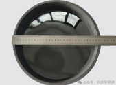
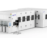
In early September, Keyou Semiconductor successfully produced a 12-inch silicon carbide ingot based on its independently developed 12-inch silicon carbide crystal growth furnace and thermal field technology. This achievement marks Keyou as one of the few semiconductor companies in China to master the complete set of core technologies for 12-inch silicon carbide crystal growth equipment and processes, achieving a comprehensive independent breakthrough from equipment to materials.
12-inch wafers first appeared
This breakthrough not only reflects Keyou's continuous innovation capabilities in silicon carbide crystal growth technology and thermal field design, but also the company's self-developed equipment and independent process are important proof of its solid technical strength in the field of wide bandgap semiconductor materials.
As a third-generation semiconductor material, silicon carbide is a key foundational material for emerging national strategic industries such as new energy vehicles, 5G communications, and rail transit. In recent years, with the rapid development of emerging fields such as artificial intelligence and wearable devices (such as AR glasses), silicon carbide's performance advantages, such as high frequency, high power, and high temperature resistance, have become even more prominent.
The area of a 12-inch substrate is about 2.25 times that of an 8-inch substrate, which means that the number of chips for AR glasses that can be produced by a single 12-inch substrate is much higher than that of an 8-inch substrate. In large-scale production, this can significantly reduce the unit cost of crystal growth, processing, polishing and other links, and is a key path to reducing the cost of core components of AR glasses.
