Chinese semiconductor thread II

tokenanalyst

Brigadier
Registered Member

Jingcun's subsidiary, Miaocun Technology, releases its new blockbuster QLC NAND UFS 2.2 storage​

As smart devices continue to pursue high performance and large capacity, QLC NAND UFS memory is becoming a focus of industry attention. Compared to traditional TLC architecture, QLC offers higher storage density and a more cost-effective price, but it also places higher demands on storage controllers and firmware.
821527ac78242db8fa8d87071f9d28de.png

Building on its long-term experience and R&D investment in controller chip technology, Jingcun Technology, a subsidiary of Jingcun, has launched its new QLC NAND UFS 2.2 storage product . Notably, Miaocun Technology pioneered the release of UFS controllers and modules at the end of last year. This new product launch aims to provide the end market with a storage solution that combines high performance with high cost-effectiveness.

Relying on independently developed controller technology and continuously optimized firmware solutions, Miaocun Technology's QLC NAND UFS 2.2 memory achieves a precise balance between capacity and performance, with excellent performance and stable operation capabilities. It can better unleash the potential of QLC NAND and meet the needs of terminal devices in diverse scenarios such as system startup, application loading, and interactive response.

MiCun Technology's QLC NAND UFS 2.2 Memory Core Advantages
01 Self-developed controller + customized firmware optimization
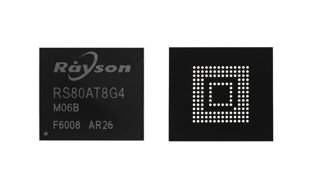
Equipped with the self-developed UFS controller chip ATM102, it conducts in-depth analysis of QLC NAND characteristics and optimizes the firmware design by combining software and hardware.

Customized firmware can effectively improve QLC NAND's read and write efficiency, lifespan, and energy consumption, ensuring product stability and reliability.
02 Excellent performance, far exceeding eMMC
The comprehensive performance of QLC NAND UFS 2.2 memory is about three times that of eMMC, the price is close to that of eMMC, and it is superior to TLC UFS 2.2 in some indicators.​
  • Sequential read >900MB/s
  • Sequential write speed >800MB/s
  • Random read and write speeds can exceed 500MB/s, and some indicators are even better than TLC NAND UFS 2.2 products.
03 Flexible capacity selection
Currently, the products cover three capacity segments: 128GB, 256GB, and 512GB. In the future, we will further launch 1TB and 2TB ultra-large capacity products to meet the diverse needs from mid-range to high-end devices.
04 Wide range of application scenarios
The product is suitable for consumer electronic terminals such as smartphones and tablets, and is compatible with mainstream control platforms, providing OEM manufacturers with an ideal storage solution with large capacity, high cost performance and high performance.

Please, Log in or Register to view URLs content!
 

tokenanalyst

Brigadier
Registered Member

Harbin Institute of Technology team: New progress in diamond Schottky diode research.​


The "Diamond Isotope Battery Technology" developed by the Optoelectronic Thin Film and Crystal Team of Harbin Institute of Technology won the Jury's Special Commendation Gold Award. This award, known as the "gold of golds," requires a unanimous vote and is extremely valuable.

The winning project focused on optimizing the performance of diamond isotope batteries. The team proposed a novel strategy for introducing an ultrathin TiO₂ layer into the diamond Schottky diode structure, effectively increasing the interface barrier height and improving the energy conversion efficiency of the radiovoltaic effect. Experimental results showed that the improved battery achieved high open-circuit voltages of 1.7 V and 1.8 V under irradiation with americium-241 and deuterium lamps, respectively, and significantly improved short-circuit current density, resulting in overall performance far exceeding that of conventional devices.

The related results , titled " Enhancement of open-circuit voltage of diamond voltaic battery by surface passivation, " were published in the internationally recognized journal IEEE Transactions on Nuclear Science. The paper is co-first authored by Zuo Yiyong and Li Chuanlong from the School of Aeronautics and Astronautics at Harbin Institute of Technology, with Associate Professor Liu Benjian as the corresponding author. This breakthrough not only sets a new performance record for diamond energy converters but also opens up new avenues for future applications in spacecraft, MEMS devices, and self-powered sensors.​

1757430435842.png1757430453071.png
1757430481596.png

Please, Log in or Register to view URLs content!
 

tokenanalyst

Brigadier
Registered Member

Nanjing Huatian Advanced Packaging Co., Ltd. was officially established with a registered capital of 2 billion yuan.​

Nanjing Huatian Advanced Packaging Co., Ltd. completed its industrial and commercial registration and was officially established.
According to information, Nanjing Huatian Advanced Packaging Co., Ltd. was jointly established by Huatian Technology (Jiangsu) Co., Ltd. and Huatian Technology (Kunshan) Electronics Co., Ltd., both wholly-owned subsidiaries of Tianshui Huatian Technology Co., Ltd., and its wholly-owned subsidiary, Huatian Advanced No. 1 (Nanjing) Equity Investment Partnership (Limited Partnership). The company's legal representative is Xiao Zhiyi, and its registered capital is 2 billion yuan.

According to previous reports from Nanjing Daily, Huatian Technology announced the integration of its three core divisions - Huatian Technology (Jiangsu) Co., Ltd., Huatian Technology (Kunshan) Electronics Co., Ltd., and Huatian Advanced No. 1 (Nanjing) Equity Investment Partnership (Limited Partnership), and invested 2 billion yuan to establish Nanjing Huatian Advanced Packaging Co., Ltd. (hereinafter referred to as "Huatian Advanced") in Pukou Economic Development Zone.

Zhu Yuping, deputy general manager of Huatian Technology (Nanjing) Co., Ltd., introduced: "Purely domestically produced 2.5D/3D advanced packaging and testing technology is still blank in China. What Huatian's domestic production line is doing is to make breakthroughs from scratch, especially in the reliability, yield, stability and other aspects of high-end plastic packaging materials, in order to reduce dependence on foreign materials and equipment and avoid being "choked." Huatian Technology has done a lot of preliminary preparation work. The imported line is now running smoothly in the second quarter. In the second half of the year, the construction and debugging of the domestic line will be completed, and small-batch sample testing will be carried out.

Please, Log in or Register to view URLs content!
 

tphuang

General
Staff member
Super Moderator
VIP Professional
Registered Member
Please, Log in or Register to view URLs content!

高功率电子设备:

金刚石上氮化镓金刚石上碳化硅器件为功率放大器、射频发射器和功率转换器实现了卓越的热性能。


量子技术:

NV 中心金刚石晶片由于其较长的电子自旋相干时间,对于量子计算、量子传感和磁力测量至关重要。


高频射频设备:

金刚石基板
可最大限度地减少射频损耗,同时控制雷达和电信系统中高功率信号产生的热量。


光学元件:

金刚石窗口和透镜可承受高激光强度和恶劣的化学环境。

热管理:金刚石散热器集成到微电子器件中,以防止过热并延长设备寿命。
some of the primary usage for diameter wafers. As substrate for GaN and SiC in high power electronics as power amplifiers and RF transmitter and power converters.

Very useful in radar & telecom equipment for medium to high power communication due to conductivity and low energy loss

Used in quantum computing, and other quantum field.

used in optical components and can handle laser strength.

thermal management used as heat sink in ICs.
 

tphuang

General
Staff member
Super Moderator
VIP Professional
Registered Member
Please, Log in or Register to view URLs content!

在5G/6G通信、毫米波雷达(24GHz以上)及AI算力芯片等高需求应用的强劲驱动下,集成无源器件(IPD)技术在滤波器、双工器、功分器、衰减器、耦合器等关键无源元件中的应用日益广泛。相较于传统硅基板,玻璃基板凭借其低介电损耗、高热稳定性、高电阻率、可调热膨胀系数等卓越材料特性,为无源器件提供了更高性能、更高集成度的理想平台。


云天半导体凭借在玻璃通孔(TGV)技术领域的深耕与突破, 专注于TGV及其相关工艺的持续创新,研发推出了覆盖广泛应用的玻璃基IPD器件,为5G/6G通信、毫米波雷达、高速互联等前沿应用提供了核心无源解决方案,填补了国内高端无源器件领域的多项技术空白。
Yuntian semiconductor using TGV tech to develop glass based IPD component for 5G/6G communication, MMW radar, high speed communication, RF filters and more. this is for 24GHz+ and AI computing chips.
 

sunnymaxi

Major
Registered Member
but a very low domestic market share in inspection & metrology (4%). The latter actually has a lot of domestic firms, but they are all very small.
sir, this section of article have so many mistakes and have outdated data.. author just randomly gave the percentage without even mention a single domestic company and their official report.

there are at least 5-6 big domestic companies in inspection field in order to compete with different KLA tools. and delivered tools in advanced category. i believe 2024-25 market share of domestic firms will be totally different once report come out.

1. Jingce Electronics:-

The company's semiconductor inspection business is developing rapidly, with orders in the semiconductor field of about 1.602 billion yuan.

Jingce Electronics' products for semiconductor front-end measurement equipment include film thickness measurement systems, optical critical dimension measurement systems, electron beam defect detection systems, semiconductor silicon wafer stress measurement equipment, and bright-field optical defect detection equipment. Some of the company's main products have completed the delivery and acceptance of 7nm advanced processes, and products with more advanced processes are currently being verified.

Some main products have completed the delivery and acceptance of 7nm advanced process. on August 12, 2023. The company signed a formal order with a customer for bright field defect detection equipment for the 14nm advanced process node.

this company also decisively broke KLA monopoly in Optical Critical Dimension measuring equipment. delivered equipment to one of the key domestic customer.

121212.jpg

2. Skyverse-

2023 annual report. Revenue up 75% yoy. Very complete lineup of optical metrology/inspection tools

111.jpg
---------------------------------------------------------------------------------------------------------------------------------------------------
3. Nano -

DF70, which is positioned for dark field inspection of graphic wafers, is benchmarked against the KLA Voyager series and uses deep ultraviolet DUV lasers. It can be applied to 12-inch advanced process production lines, filling the gap in the advanced process field for domestic manufacturers.

1741986978972.png

Nano's DF product series will not only meet the production line requirements of the 7nm node, but will also be compatible with the production line requirements of the 28nm-10nm node, competing with the KLA PUMA series and achieving a comprehensive replacement of KLA products in the field of dark field inspection of graphic wafers.
----------------------------------------------------------------------------------------------
4. Zhongke Feice

Zhongke Feice: Bright field nano-pattern wafer defect inspection equipment has been shipped in small batches.​


the bright-field nano-pattern wafer defect detection equipment has been shipped in small batches; its dark-field nano-pattern wafer defect detection equipment has been shipped to some customers' production lines for process development and application verification; the optical critical dimension equipment currently has good verification results on the client side, and is undergoing corresponding testing for delivery to the customer's mass production department." In particular, the investment in bright-field and dark-field equipment is very large. The goal is to complete the verification of the equipment in the customer's production line as quickly as possible and complete localized replacement. "

Chen Lu added.Regarding the current market demand performance of the company's semiconductor quality control equipment, Gu Kainan, director and secretary of the board of directors of China Science and Technology Testing, said that benefiting from the continuous expansion of production capacity of domestic wafer fabs, the domestic semiconductor equipment industry is in a period of rapid development.It is worth mentioning that in recent years, applications such as AI and computing chips have brought many technological innovations to integrated circuit manufacturing, including 2.5D and 3D packaging used in HBM. These process innovations have also put forward higher requirements for detection and measurement equipment.


wafer defect detection tool:
View attachment 139885

CD measurement tool
View attachment 139886
Please, Log in or Register to view URLs content!
Metrology is the fastest growing sector right now..

Different from what some stooges think, metrology is one the fastest growing equipment sectors in China.

Tianjue Technology (TZTEK): China's first 40NMBFI released, semiconductor layout ushered in new breakthroughs​


Tianjue Technology announced on its official account that Suzhou Sihang Semiconductor Technology Co., Ltd. (hereinafter referred to as "Sihang Semiconductor"), in which it holds a stake, has completed in-factory verification of its bright-field nano-pattern wafer defect detection equipment TB1500 for the 40nm technology node, marking a new breakthrough in domestic high-end semiconductor detection equipment.

  Defect detection equipment is an important tool for chip quality improvement, cost reduction, and iteration: In chip manufacturing, from the entire wafer to a single chip, defect detection equipment is an important tool for chip quality improvement, cost reduction, and iteration. The

  TB1500 announced this time is another breakthrough following the TB1000 in August last year. All core key components are independently controllable. At the same time, advanced signal processing algorithms are used to effectively improve the signal-to-noise ratio and detection sensitivity to meet the process requirements of the 40nm technology node. The TB2000 equipment for the 28nm technology node is currently progressing smoothly, and all core components have been developed. It is planned to release a prototype by the end of 2024.

  The semiconductor layout has blossomed in many places, and the new product iteration of wholly-owned subsidiaries has also progressed smoothly: the DaVinci G5 equipment developed by wholly-owned subsidiary MueTec for the 12-inch 40nm technology node has been verified by a large amount of wafer actual measurement data and has performed well. The equipment improves the repeatability, throughput and high aspect ratio overlay mark recognition capabilities, making it possible to detect the overlay accuracy of complex chip patterns and improving manufacturing efficiency.

View attachment 133789

Please, Log in or Register to view URLs content!

Metrology from SMEE...2.png

there are more prominent domestic companies in Metrology sector. and at the end, we have Sicarrier too. they announced 2nd production base in Shanghai to produce tools for advanced process in early next year.
 
Top