You are using an out of date browser. It may not display this or other websites correctly.
You should upgrade or use an alternative browser.
You should upgrade or use an alternative browser.
Chinese semiconductor thread II
- Thread starter vincent
- Start date
Domestic robot joint modules adopt GaN, with a target shipment of 20,000-30,000 units
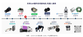
Xinhua Finance reported that another domestic humanoid robot-related company adopted a gallium nitride solution in its servo drive .It is understood that Suzhou Zhuoyu Electric Technology Co., Ltd. and its subsidiary Beijing Zhuoyu Technology Co., Ltd. focus on embodied intelligent core drive components, and independently develop core components of humanoid robots such as planetary joint modules, harmonic joint modules, linear actuators, frameless torque motors, servo drives, and planetary reducers. Among them, the entire series of servo drives adopts gallium nitride solutions with high power density and low heat generation.
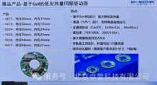
Zhuoyu Electric said that this servo drive adopts a large hollow design and high power density design to meet the requirements of the robotics industry. It is not only developed based on GaN power devices, but also highly integrates the driver chip and force control chip into one, with a maximum power of 17KW (100A/200V).
MatrixTime Robotics expanding its inspection equipment offerings for more semiconductor process and incorporating more AI based defect detection automation.
Jushi Technology offers the Juxin 6500 advanced process unpatterned wafer dark-field defect inspection system, suitable for advanced fab processes, large silicon wafers, and Gen3.5 substrates and epitaxial wafers . This dark-field nano-level defect inspection system covers advanced process inspection needs. For CMP/etching/development processes, Gen3.5 SiC/GaN, large silicon wafers, and MicroOLEDs, the Juxin 6300 high-sensitivity wafer process defect inspection system boasts extremely small defect recognition capabilities and strong process adaptability. The system features an embedded AI large-model ADC system, enabling high detection capabilities and complete system intelligence.
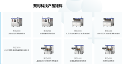
With the popularization of technologies such as chiplets and 3D packaging, advanced packaging has placed higher demands on AOI equipment. Jushi Technology's current main products, the Juxin 3000/3300, implement LeadScan 2D/3D defect detection and measurement for IC chips and components, covering 6S LeadScan full inspection of all types of chips such as BGA/QFP/QFN/SiP/Chiplet . For quality control in final inspection and process inspection, it is widely used in quality inspection and unmanned automated defect analysis after semiconductor packaging and electrical testing and before shipment. In addition, the Juxin 3700 product is designed for 2D/3D diebond/wirebond processes and automotive-grade chip process inspection . This equipment has a self-developed 3D inspection module solution, a self-developed large field of view and high-pixel optical and mechanical system, and multi-threaded data algorithms, resulting in industry-leading productivity. Currently, the entire Juxin 3000 product line has been introduced into mass production.
Jushi Technology offers the Juxin 6500 advanced process unpatterned wafer dark-field defect inspection system, suitable for advanced fab processes, large silicon wafers, and Gen3.5 substrates and epitaxial wafers . This dark-field nano-level defect inspection system covers advanced process inspection needs. For CMP/etching/development processes, Gen3.5 SiC/GaN, large silicon wafers, and MicroOLEDs, the Juxin 6300 high-sensitivity wafer process defect inspection system boasts extremely small defect recognition capabilities and strong process adaptability. The system features an embedded AI large-model ADC system, enabling high detection capabilities and complete system intelligence.

With the popularization of technologies such as chiplets and 3D packaging, advanced packaging has placed higher demands on AOI equipment. Jushi Technology's current main products, the Juxin 3000/3300, implement LeadScan 2D/3D defect detection and measurement for IC chips and components, covering 6S LeadScan full inspection of all types of chips such as BGA/QFP/QFN/SiP/Chiplet . For quality control in final inspection and process inspection, it is widely used in quality inspection and unmanned automated defect analysis after semiconductor packaging and electrical testing and before shipment. In addition, the Juxin 3700 product is designed for 2D/3D diebond/wirebond processes and automotive-grade chip process inspection . This equipment has a self-developed 3D inspection module solution, a self-developed large field of view and high-pixel optical and mechanical system, and multi-threaded data algorithms, resulting in industry-leading productivity. Currently, the entire Juxin 3000 product line has been introduced into mass production.
Defect density and overlay are complete showstoppers.Surpassing Japan! China delivers its first nanoimprint lithography machine: line width less than 10nm
GalaxyCore: The company's 0.61-micron 50-megapixel image sensor product has achieved mass production and shipment
GalaxyCore announced the recent mass production and shipment of its 0.61-micron, 50-megapixel image sensor. This product, the world's first single-chip 0.61-micron pixel image sensor, is based on the company's proprietary Galaxy Cell® 2.0 process platform and manufactured in its own wafer fab, significantly improving small-pixel performance.
The product utilizes a 1/2.88 optical aperture, reducing the thickness of camera modules and making it widely applicable to smartphone rear-mounted main cameras, ultra-wide-angle cameras, and front-facing cameras. It also integrates single-frame high dynamic range (DAGHDR) technology, achieving a wider dynamic range in a single exposure, effectively addressing over- and underexposure issues in backlit scenes. It also supports PDAF (phase autofocus), ensuring a fast and accurate shooting experience.
GalaxyCore stated that the company's 0.61-micron 50-megapixel image sensor has entered mass production and shipment, successfully entering the rear-mounted main camera market for branded mobile phones. This marks further market recognition of the company's innovative high-pixel single-chip integration technology and fully demonstrates the efficiency of its Fab-Lite model. To date, the company has achieved mass production of 0.7-micron 50-megapixel, 1.0-micron 50-megapixel, and 0.61-micron 50-megapixel image sensors based on single-chip integration technology.
Subsequently, the company will further iterate the performance of high-pixel products such as 32 million and 50 million based on this technology platform, and at the same time launch higher-specification products with more than 100 million pixels, continuously enhancing the company's core competitiveness, increasing market share and expanding its leading edge.
Maybe a showstopper for logic node manufacturers, it will take them some time to adopt NIL. But memory makers in Japan had been in the NIL train for quite some time.Defect density and overlay are complete showstoppers.
Prinano has been trying to make their tools for semiconductor manufacturing along Tianren Nano who has been trying to get their tools into MRAM manufacturing.
4) Cooperate with GermanLitho/Tianren Micro-Nano Technology and Leuven Instrument industry-university-research institute to jointly develop special equipment focusing on magnetic sensor array/MRAM 2/4/6/8-inch nanoimprinting and 8/12-inch RIE/IBE dual engraving Etching technology exclusive etching equipment for magnetic materials.
Saiwei Microelectronics starts trial production of the first batch of MEMS silicon crystal oscillator 8-inch wafers
Saiwei Semiconductor issued an announcement stating that recently, a MEMS (abbreviation of Micro-Electro-Mechanical Systems) silicon crystal oscillator manufactured by the company's controlling subsidiary Saiwei Microsystems Technology (Beijing) Co., Ltd. (hereinafter referred to as "Saiwei Beijing") has passed customer verification. Saiwei Beijing has received a purchase order from the customer and started small-batch trial production of the first batch of MEMS silicon crystal oscillator 8-inch wafers.
Founded in 2008, Saiwei Microelectronics' main products and businesses include process development and wafer manufacturing for MEMS chips, as well as GaN epitaxial material growth and device design. The company manufactures a variety of MEMS chips, including silicon photonics, micro-vibration mirrors, and silicon microphones, as well as RF passive components and modules manufactured using MEMS integration processes. These products are widely used in a variety of fields, including communications, biomedical, industrial automotive, and consumer electronics.
The MEMS silicon oscillator is a new type of frequency control device manufactured based on microelectromechanical systems (MEMS) technology. It generates stable frequency signals through micro-mechanical vibrations of silicon-based materials. It has widely replaced traditional quartz crystal oscillators and has become a core component of the "time reference" in electronic devices. Unlike traditional quartz crystal oscillators, which rely on the piezoelectric effect of the quartz crystal, the vibration source of MEMS silicon oscillators is the silicon material itself, making them more compatible with CMOS integrated circuits and enabling "chip-level" integration
More about the PriNano NIL tool news:
PriNano first stepper nanoimprint lithography system delivered!
According to the WeChat official account of "Pulin Technology", on August 1, 2025, the first PL-SR series inkjet stepper nanoimprinting equipment independently designed and developed by PuLin Technology successfully passed the acceptance and was delivered to domestic specialty process customers.
PuLin Technology said: "This equipment delivery is a new milestone for our business expansion and market penetration, marking a solid step forward for our company in the field of high-end semiconductor equipment manufacturing."
It is reported that the PL-SR series inkjet stepper nanoimprint equipment has overcome key technical difficulties such as non-vacuum complete bonding of stepper hard boards, spray glue and thin glue imprinting, and control of the residual layer of imprint glue. It can correspond to nanoimprint lithography processes with line widths of less than 10nm.
By comparison, Canon's previously released FPA-1200NZ2C nanoimprint lithography system can achieve 14nm linewidths through nanoimprint technology, enabling it to claim to be capable of producing 5nm process chips. PuLin Technology's PL-SR series inkjet stepper nanoimprint lithography system surpasses Canon in this regard. However, this does not mean that PuLin Technology's PL-SR series inkjet stepper nanoimprint lithography system can be used to manufacture advanced 5nm process logic chips.
Compared with the currently commercialized EUV lithography technology, although the use of nanoimprint technology to manufacture chips does not require a complex EUV light source system, it can significantly reduce energy consumption and equipment costs (according to Canon, power consumption can be reduced to 10% of EUV technology, and equipment investment can be reduced to 40% of EUV equipment alone), but its chip manufacturing speed is slower than traditional lithography methods and is not suitable for chip manufacturing with complex logic processes.
Because the internal graphics structure of logic process chips is complex, with dozens of different layers of circuit structures, this means that a new imprint head needs to be replaced for each layer of graphics. This not only makes the process more complicated, but also greatly reduces manufacturing efficiency and leads to a significant increase in costs (a large number of nanoimprint heads are required to pattern the different internal layers of the chip). In contrast, the graphics of memory chips such as NAND Flash are simpler because they are stacked with multiple nearly identical layers, making them more suitable for nanoimprint technology processes. This also means that domestic memory chip manufacturers have the hope of improving their process technology by utilizing domestic nanoimprint equipment, breaking the Western blockade of China's high-end memory manufacturing equipment and better competing with memory giants such as SK Hynix and Samsung.
According to PuLin Technology, its PL-SR series inkjet stepper nanoimprint lithography equipment is equipped with a proprietary template profile control system, nanoimprint photoresist inkjet algorithm, inkjet printing material matching, and a proprietary software control system. This equipment has already completed preliminary R&D and verification for memory chips, silicon-based microdisplays, silicon photonics, and advanced packaging.
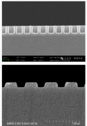
The PL-SR series has successfully overcome several technical bottlenecks in the inkjet coating process, achieving a major breakthrough in spray-type nanoimprint lithography materials. In semiconductor-level chip imprint processes, chip structures typically feature nanostructures with variable duty cycles and multi-cycle variations. This complex structural design requires precise control of the local adhesive volume, dynamically adjusting the amount of adhesive sprayed based on structural changes to achieve a thin and consistent residual layer thickness. Through innovative material formulations and process control, the PL-SR series improves adhesive droplet density and spread, successfully achieving nanometer-scale imprint film thicknesses, with an average residual layer of less than 10nm, residual layer variation of less than 2nm, and an imprinted structure aspect ratio greater than 7:1. The company has developed multiple nanoimprint adhesive systems that are compatible with the spray-type step imprint process and subsequent semiconductor processing. In particular, it has developed solvent-cleanable, photocurable nanoimprint adhesives, addressing the potential risk of expensive quartz templates being contaminated by residual adhesive and providing reliable material support for high-precision step nanoimprinting.
They are not the only ones, there is more companies trying to get into the NIL stepper market:
Like Istar NIL steppers:
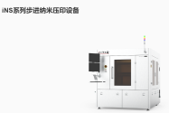
Tianren Nano NIL tools that can achieve 100 WPH, 10nm resolution, 10:1 ratios and have nanometer level overlay but is not an stepper.


If is good for Gigaphoton is good for Beijing RSLaser.
CSIC Special Gas: Photolithography gas products have been certified as qualified suppliers by Japan's GIGAPHOTON Co., Ltd.
China Shipbuilding Special Gases Co., Ltd. issued an announcement stating that the company recently received a qualified supplier certification certificate from Japan's GIGAPHOTON Co., Ltd. (hereinafter referred to as "GIGAPHOTON"). The company's photolithography gas products (Kr/Ne, Ar/Ne/Xe) have passed GIGAPHOTON's qualified supplier certification, and the certificate is valid until July 23, 2030.
Founded in 2000 and headquartered in Oyama City, Tochigi Prefecture, Japan, GIGAPHOTON Co., Ltd. is a leading company in the semiconductor lithography field, specializing in the development and manufacture of excimer lasers, deep ultraviolet (DUV), and extreme ultraviolet (EUV) light sources for lithography. Leveraging its proprietary laser and optical measurement technologies, the company provides high-performance lithography light source solutions to semiconductor manufacturers worldwide. In recent years, GIGAPHOTON has not only gained traction with nearly all semiconductor manufacturers in the Asian market, including Japan, but has also achieved rapid growth in the European and American markets.
CSIC Special Gases stated that its GIGAPHOTON certified supplier for photolithography gas products (Kr/Ne, Ar/Ne/Xe) demonstrates that its products meet the stringent requirements of international high-end semiconductor manufacturing in terms of core performance indicators such as purity and stability. This certification is a significant recognition of the company's technological R&D capabilities and product quality control system. This certification will help the company expand its business opportunities within the high-end semiconductor equipment industry chain, enhance its market competitiveness in the electronic specialty gas sector, and positively impact the company's expansion of its photolithography gas product business.
Last edited:
