Chinese semiconductor thread II

broadsword

Brigadier
The complete SCMP report of the Harbin EUV light source via Emperor of CDF. 2026 looks too optimistic though.

How China’s award-winning EUV breakthrough sidesteps US chip ban
Story by Zhang Tong • 22h • 4 min read

As US restrictions continue getting tougher, Chinese researchers are coming up with innovative approaches to chip manufacturing
New approaches in the development of extreme ultraviolet (EUV) lithography are being pioneered by Chinese scientists, paving the way for the mass production of advanced semiconductor chips as researchers race to sidestep the strict sanctions put in place by the United States.

And one such project from the Harbin Institute of Technology was recently awarded first prize at the Harbin Provincial Innovation Achievement Transformation Competition for employees in universities and research institutes on December 30.

The research team took a completely different technological approach from Western methods to generate EUV laser light.

According to the institute's website, the "discharge plasma extreme ultraviolet lithography light source" project, led by Professor Zhao Yongpeng from the school of aerospace engineering, "boasts high energy conversion efficiency, low cost, compact size and relatively low technical difficulty".

"It can produce extreme ultraviolet light with a central wavelength of 13.5 nanometres, meeting the urgent demand for EUV light sources in the photolithography market," the official report said.

In the semiconductor industry, the most complex and difficult-to-manufacture machine is the photolithography machine.

Only EUV lithography machines are capable of producing chips smaller than seven nanometres, and currently, the only company in the world that can manufacture EUV machines is Dutch firm ASML.

The US has imposed strict export controls, preventing China from acquiring EUV lithography machines and associated technologies, software and components.

Under pressure from the US, ASML has been prohibited from selling its most advanced EUV equipment to China since 2019. On January 15, the Netherlands announced an expansion of export controls on semiconductor-related items.

ASML's EUV light source relies on using high-energy lasers to bombard liquid tin droplets, creating plasma in a process known as the laser-produced plasma (LPP) method. This process involves high-energy laser components and complex FPGA chip control, with the core technology long dominated by foreign companies.

Zhao's team, on the other hand, uses the laser-induced discharge plasma (LDP) method, where a laser first vaporises a small amount of tin into a cloud between two electrodes. A high voltage is then applied across the electrodes to inject energy, converting the tin cloud into plasma. The resulting electrons and high-valence tin ions frequently collide and radiate, generating EUV light.

Compared with LPP technology, the LDP method is simpler, more cost-effective and directly converts electrical energy into plasma with higher energy utilisation efficiency.

However, optimising the parameters and timing of discharge pulses remains a significant technical challenge. Some also have concerns that LDP might struggle with power output limitations.

Since 2008, Zhao has been involved in the development of discharge plasma EUV light sources, and this recent award suggests that his team may have made new progress. Zhao declined an interview request.

EUV research is also being conducted by other Chinese teams, with multiple approaches being adopted.

A team from the Shanghai Institute of Optics and Fine Mechanics, Chinese Academy of Sciences, published details of its work in the LPP method in December 2023 in the journal Laser & Optoelectronics Progress.

Meanwhile, Professor Xuan Hongwen's team at the Guangdong Bay Area Aerospace Information Research Institute published research in April 2023 in the Chinese Journal of Lasers, focusing on enhancing LDP EUV light output power and conversion efficiency.

Additionally, Tsinghua University is leading the construction of a major national scientific infrastructure project, the SSMB-EUV, which is expected to serve as a light source for photolithography machines in the future.

Beyond the core light source system, manufacturing a complete lithography machine also requires high-precision components, such as mirrors.

On October 17, 2023, the US Department of Commerce updated its semiconductor equipment restrictions, placing specific limits on the precision of lithography machine components. In 2024, the US revised its export controls to include restrictions on EUV masks and etching machines used in manufacturing.

In January 2024, Professor Zhao's research group, in collaboration with a team led by Zhang Junyong at the Shanghai Institute of Optics and Fine Mechanics, made advances in controlling and focusing EUV light.

These developments may represent the first steps in China's long journey towards mastering photolithography technology.

Copyright (c) 2025. South China Morning Post Publishers Ltd. All rights reserved.
 

tphuang

Lieutenant General
Staff member
Super Moderator
VIP Professional
Registered Member
I'm going to have to start deleting posts again if you people keep on posting stuff with the assumption that SCMP actually knows what's going on.

Remember, light source is either from SIOM and CIOMP. We have the patent filings on that and official visit.
 

tphuang

Lieutenant General
Staff member
Super Moderator
VIP Professional
Registered Member

a rather interesting chart here showing the trajectory of China's SME import. I would say the fact that lithography increases were so much greater than etching and deposition (despite the huge expansion of memory chip capacity) would indicate just how much of the spending are toward domestic equipment.
 

tokenanalyst

Brigadier
Registered Member
I'm going to have to start deleting posts again if you people keep on posting stuff with the assumption that SCMP actually knows what's going on.

Remember, light source is either from SIOM and CIOMP. We have the patent filings on that and official visit.
SIOM is more like the general EUV optics, computational lithography, EUV Masks and Photoresist.

Please, Log in or Register to view URLs content!

CIOMP is the LPP light source. They are collaborating with other institutions like Hangzhou University.
 

Wahid145

Junior Member
Registered Member
Please, Log in or Register to view URLs content!

Screenshot_20250122_085923.jpg

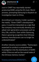
This guy is having a paranoia about CXMT as of late and it's an amazing accomplishment by that company. I'm sure CXMT is using some of the same loopholes SMIC used to import SME to develop below 18.5nm DRAM.

But really interesting to see how american administration in turning a blind eye on them.

I remember when they got the news on YMTC surpassing Samsung they were sanctioned very quickly
 

tokenanalyst

Brigadier
Registered Member

New breakthrough in diamond quantum devices!​


The world's first 800kV ultra-high voltage direct current quantum current sensor (hereinafter referred to as "quantum current sensor "), jointly developed by China Southern Power Grid Corporation's Transmission and Distribution Department, China Southern Power Grid Digital Research Institute, China Southern Power Grid Sensor Company, Shanghai Institute of Microsystem and Information Technology of the Chinese Academy of Sciences, Ultra-high Voltage Transmission Company, Guizhou Power Grid Company, Xidian High Voltage Switch, University of Science and Technology of China, Zhejiang University and other units, successfully passed the new product technical appraisal . The appraisal committee composed of Academician Li Lixuan of the Chinese Academy of Engineering, Academician Chen Yong of the Chinese Academy of Engineering, and He Jinliang, a distinguished professor of the Yangtze River Scholar Program of Tsinghua University, unanimously agreed that the comprehensive technical performance of the product has reached the international leading level, marking a major breakthrough in China's quantum precision measurement field and seizing the commanding heights of global quantum sensing technology.

Sensors are like nerve endings in the human body, sensing and generating various measurement data all the time. More and more sensors are installed in the power grid, giving it more "clairvoyance" and "clairaudience", making it more sensitive.

"The quantum current sensor is a more powerful 'sense' for the power grid. It can see farther and hear more clearly. It can accurately sense extremely weak currents at the milliampere level and measure large short-circuit currents at the tens of kiloamperes level. It can monitor the operation and health status of DC transmission lines in real time." said the relevant technical director of the State Grid Corporation of China.

Please, Log in or Register to view URLs content!
 

tokenanalyst

Brigadier
Registered Member

The first high-voltage radiation-resistant silicon carbide power device has been successfully developed and verified.​


the Institute of Microelectronics of the Chinese Academy of Sciences introduced the development of the first domestically produced high-voltage radiation-resistant silicon carbide (SiC) power device.

After more than one month of on-orbit power-on tests, the test data of the silicon carbide payload is normal, the on-orbit test and application verification of the high-voltage 400-volt silicon carbide power device has been successfully completed, and the static and dynamic parameters in the power system are in line with expectations. In Tang Yidan's view, the first phase of the silicon carbide payload's mission has been successfully completed, and the first domestically produced high-voltage 400-volt radiation-resistant silicon carbide power device has been successfully verified for its adaptability to the space environment and its on-orbit application in the power system. This indicates that under the demand for space payloads measured in "grams", silicon carbide power devices will become the preferred solution for significantly improving the efficiency of space power supplies, and are expected to drive the upgrading of space power systems.

Liu Xinyu pointed out that China has successfully developed the first domestically produced high-voltage 400-volt radiation-resistant silicon carbide power device, passed space verification and realized its in-orbit application in the power supply system. This will provide a new generation of power devices to choose from for China's future lunar exploration, manned lunar landing, deep space exploration and other fields, and provide strong support for China to build a world space science power.​

Please, Log in or Register to view URLs content!
 

tokenanalyst

Brigadier
Registered Member

Shanghai Microelectronics (SMEE) "Vibration Reduction Device and Semiconductor Equipment" patent is authorized​

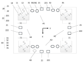
Shanghai Micro Electronics Equipment (Group) Co., Ltd. recently obtained a patent called "Vibration Damping Device and Semiconductor Equipment", with the authorization announcement number CN222122116U, the authorization announcement date is December 6, 2024, and the application date is December 29, 2023.

1737559215471.png

The utility model relates to the field of semiconductor technology, and provides a vibration reduction device and semiconductor equipment, wherein the vibration reduction device includes: at least three air spring assemblies and an actuator assembly; the air spring assembly includes a vertical air spring and a horizontal air spring, the vertical air spring is used to provide vertical support and vibration reduction, and the horizontal air spring is used to provide horizontal support and vibration reduction; the actuator assembly includes a vertical linear motor and a horizontal linear motor, the vertical linear motor is used to provide vertical vibration reduction, and the horizontal linear motor is used to provide horizontal vibration reduction. Through the combination of the above passive vibration reduction and active vibration reduction, the problem of large dynamic changes and strong variability of vibration-sensitive components of semiconductor equipment is solved, and at the same time, the problem that the vibration reduction element on the semiconductor equipment can only play a damping and vibration reduction role on a specific narrow frequency band vibration and cannot effectively suppress low-frequency vibration is solved.

Please, Log in or Register to view URLs content!
 

tokenanalyst

Brigadier
Registered Member

Park E-Jing received hundreds of millions of yuan in Series B financing to expand ultra-high purity polymer material production lines, etc.​


Pu Enjing New Energy Materials (Shanghai) Co., Ltd. (hereinafter referred to as "Pu Enjing") recently completed a round B financing of hundreds of millions of yuan. This round of financing was led by Guoke Dongfang, followed by Da Linghaowan Ceyuan Fund, Shangyan Xingong Fund, Minsheng International, Sequoia China, Shanghai Lianhe Investment, and Lianxin Capital. This round of funds will be used to expand Pu Enjing's ultra-high purity polymer material production line , upgrade the technology platform, and expand the market.
Since its establishment in November 2021, Pu Enjing has been deeply engaged in the independent research and development of high-end polymer materials. It has now broken through key technical barriers such as catalysts, polymerization processes, and application scenario development, and has taken the lead in advancing into the high-scarcity field. The company has built a rich product matrix around the ultra-high purity polymer technology platform and has developed a series of ultra-high purity polymer products for lithium battery separators, special fiber materials, medical materials, high-end filter materials in the semiconductor chip industry, and high-end polymer materials for humanoid robots.
Taking high-performance lithium battery separator materials as an example, the 9μm, 7μm, and 5μm ultra-high-purity special materials developed by Park Enjing are already in the leading position in the industry.
It is reported that Pu Enjing's "Ultra-high-purity Polymer Materials Project for New Energy" was listed as a major project in Shanghai in 2024. This is one of the world's largest ultra-high-purity high-molecular-weight polyethylene projects and one of the largest private investment projects in Shanghai last year. The project is located in Shanghai Chemical Industry Park. After full production, it will achieve an annual production scale of 280,000 tons of ultra-high-purity high-molecular-weight polyethylene. By then, Pu Enjing will fully cover new energy lithium battery separators, special fiber materials, medical materials, high-end filter materials for the semiconductor chip industry, and high-end polymer materials for humanoid robots.

Please, Log in or Register to view URLs content!
 
Top