Chinese semiconductor thread II

tokenanalyst

Brigadier
Registered Member

Xinshang Micro-Equipment successfully delivered its 500th stepper lithography machine​


On August 8, 2025, Shanghai Chip Micro-Equipment Co., Ltd. (AMIES) held a delivery ceremony for its 500th stepper. This ceremony fully demonstrated AMIES's independent innovation capabilities as a leading domestic stepper lithography company and marked a new milestone for my country's high-end semiconductor equipment industry. Leaders from relevant government departments, strategic customers, shareholder representatives, industry associations, and partner universities attended the ceremony.

AMIES's flagship product, advanced packaging lithography systems, boast high resolution, high overlay accuracy, and a large exposure field of view. They also offer robust warpage and thick-resistance handling capabilities, allowing for flexible configuration based on specific customer process requirements. These products meet the requirements of advanced packaging technologies such as flip-chip, fan-in, fan-out WLP/PLP, and 2.5D/3D.

The 500th stepper shipped this time will be delivered to Shenghe Jingwei Semiconductor (Jiangyin) Co., Ltd. Shenghe Jingwei is a global leader in advanced wafer-level integrated circuit packaging and testing. It is dedicated to supporting a wide range of high-performance chips, particularly graphics processing units (GPUs), central processing units (CPUs), and artificial intelligence (AI) chips. Through heterogeneous integration that surpasses Moore's Law, it achieves comprehensive performance improvements in high computing power, high bandwidth, and low power consumption. In recent years, Shenghe Jingwei has continuously strengthened independent innovation and focused on developing advanced 3DIC processing and integration technologies, achieving leapfrog development while also promoting the overall level of the advanced integrated circuit manufacturing industry chain.

Shenghe Jingwei has a good cooperation foundation with AMIES. It highly appreciates AMIES's product performance, technical strength and service awareness, and expresses its willingness to further deepen strategic cooperation with AMIES to jointly promote advanced packaging technology innovation and industrial development.

Please, Log in or Register to view URLs content!
 

tokenanalyst

Brigadier
Registered Member

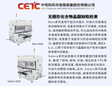
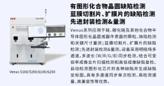
CETC Defect Detection Tools for 3rd Generation Semiconductors.​


1754760286150.png1754760321217.png

CETC Fenghua focuses on new energy vehicles, microwave communications, artificial intelligence, and advanced packaging. Targeting semiconductor materials and devices such as silicon, silicon carbide, gallium nitride, gallium oxide, gallium arsenide, and indium phosphide, it has developed a technology system combining advanced optical inspection with artificial intelligence algorithms and big data analysis and management. The company is committed to localizing defect detection equipment for key links in the industry chain, from substrate to epitaxy to chip to packaging. Its product portfolio includes both non-patterned and patterned defect inspection equipment for compound semiconductors (silicon carbide, gallium nitride, gallium arsenide, indium phosphide, lithium niobate, sapphire, and infrared materials), Si-based integrated circuits (silicon epitaxy for slip line inspection, grain size inspection, and surface defect detection such as scratches), and advanced packaging (TGV+RDL). Compatible with 4, 6, 8, and 12-inch wafers, as well as other non-standard sizes, its equipment is currently in use by over 30 industry enterprises and research institutes, contributing to the independent and controllable development of my country's semiconductor industry.

Please, Log in or Register to view URLs content!
 

def333

New Member
Registered Member
It will take about 1.5-2 years to enter industrial trial production, and complete mass production will take 28 years. There are now many process optimizations being done.

Some say that domestically produced EUV lithography machines had already begun trial production by the end of 2024.
 

horse

Colonel
Registered Member
Year 2028?

That I flatly do not believe.

It is the Chinese communist official, and if there is a date set, usually it always is delivered, what the promise or goal was, way ahead of time, that way everyone looks good and gets promoted.

Same old tricks as always.

2026 or 2027 at the absolute latest full scale EUV production of advanced chips.

:oops::D

Kind of means the EUV is already here.

LOL!

:cool:
 

nativechicken

Junior Member
Registered Member
Year 2028?

That I flatly do not believe.

It is the Chinese communist official, and if there is a date set, usually it always is delivered, what the promise or goal was, way ahead of time, that way everyone looks good and gets promoted.

Same old tricks as always.

2026 or 2027 at the absolute latest full scale EUV production of advanced chips.

:oops::D

Kind of means the EUV is already here.

LOL!

:cool:
Confirmed via reliable sources (details undisclosed) that the EUV prototype machine has been manufactured, installed, and debugged. Production line assembly is underway (pending peripheral equipment), with EUV parameter fine-tuning ongoing—a standard 1.5-2 year process.

Unlike DUVi, China lacks reference processes for EUV. Thus, all supporting EUV equipment requires development from scratch, justifying the 1.5-2 year timeline. Pilot production will follow—mirroring SMIC’s Kirin 9000s production status as of September 2022.

Domestic DUVi full production line verification (covering 7-5nm nodes) is expected by year-end. EUV mass production is projected for 2028 (2027 remains tentative, potentially limited to trial production for Huawei chips).

Current focus is ramping 5-7nm yields via domestic DUVi, with 7nm production costs just 15% higher than international benchmarks (not 30%).

China’s saturation development approach involves hundreds of teams optimizing DUVi/EUV production line parameters. Domestic DUVi—enhanced for 5nm via specialized modifications—now outperforms ASML’s DUVi. Key innovations include:

Overlay accuracy below 1nm achieved on one DUVi machine
Solid-state lasers (superior to ASML’s gas lasers frozen in 2002-2003 tech)
Potential integration of etching/ion implantation modules for ultra-high precision
Originally three separate teams, China’s DUVi effort has consolidated into a single entity (thousands strong). Beyond 5nm (quadruple patterning), they’re developing 3nm (sextuple patterning) as a cost-no-object contingency before EUV readiness.

Three EUV paths are being pursued concurrently. Harbin Institute of Technology’s LPP+electrical excitation approach currently matches ASML’s 250W EUV performance. US export controls remain effective—China must independently rediscover EUV process details without reference templates, inevitably slowing progress.

EUV lithography faces fundamental barriers at 2-3nm nodes. As alternatives, China explores four post-EUV pathways for advanced chips (only chiplet is publicly acknowledged; three others remain classified).
 

Tomboy

Junior Member
Registered Member
Confirmed via reliable sources (details undisclosed) that the EUV prototype machine has been manufactured, installed, and debugged. Production line assembly is underway (pending peripheral equipment), with EUV parameter fine-tuning ongoing—a standard 1.5-2 year process.

Unlike DUVi, China lacks reference processes for EUV. Thus, all supporting EUV equipment requires development from scratch, justifying the 1.5-2 year timeline. Pilot production will follow—mirroring SMIC’s Kirin 9000s production status as of September 2022.

Domestic DUVi full production line verification (covering 7-5nm nodes) is expected by year-end. EUV mass production is projected for 2028 (2027 remains tentative, potentially limited to trial production for Huawei chips).

Current focus is ramping 5-7nm yields via domestic DUVi, with 7nm production costs just 15% higher than international benchmarks (not 30%).

China’s saturation development approach involves hundreds of teams optimizing DUVi/EUV production line parameters. Domestic DUVi—enhanced for 5nm via specialized modifications—now outperforms ASML’s DUVi. Key innovations include:

Overlay accuracy below 1nm achieved on one DUVi machine
Solid-state lasers (superior to ASML’s gas lasers frozen in 2002-2003 tech)
Potential integration of etching/ion implantation modules for ultra-high precision
Originally three separate teams, China’s DUVi effort has consolidated into a single entity (thousands strong). Beyond 5nm (quadruple patterning), they’re developing 3nm (sextuple patterning) as a cost-no-object contingency before EUV readiness.

Three EUV paths are being pursued concurrently. Harbin Institute of Technology’s LPP+electrical excitation approach currently matches ASML’s 250W EUV performance. US export controls remain effective—China must independently rediscover EUV process details without reference templates, inevitably slowing progress.

EUV lithography faces fundamental barriers at 2-3nm nodes. As alternatives, China explores four post-EUV pathways for advanced chips (only chiplet is publicly acknowledged; three others remain classified).
Pardon me for my question, but will Chinese foundries capable of producing top end nodes comparable to the latest TSMC/Samsung processes once EUV machines become fully operational in 2027/2028? I've read in this thread that 3nm nodes has already been developed but is pending EUV machines to mass produce but nothing on more advanced nodes like 2nm and TSMC A14 equivalent (According to roadmaps TSMC tends to produce these by 2027).
 

nativechicken

Junior Member
Registered Member
The current state of domestic EUV development roughly matches where domestic DUVi stood in 2021—capable of etching high-precision patterns, equivalent to equipment validation/testing.

After 1.5-2 years of production line debugging, by late 2026 to early 2027, preliminary EUV production processes will be finalized with equipment fully integrated into production lines. This enables pilot production—similar to SMIC South’s Kirin 9000s production for Huawei in September 2022—characterized by initial low yields and ongoing process refinement.

By late 2028, target yields should reach commercially viable levels with optimized production lines. Domestic EUV systems will commence scaled deployment, mirroring the rollout schedule of domestic DUVi memory chip production lines in late 2025.

Timelines are realistically fixed given systemic complexity. Accelerating progress isn’t feasible through hundreds working overtime—it demands industry-wide round-the-clock efforts for multiple years to overcome the West’s 10-15-year cumulative advantage.
 

AsuraGodFiend

New Member
Registered Member
The current state of domestic EUV development roughly matches where domestic DUVi stood in 2021—capable of etching high-precision patterns, equivalent to equipment validation/testing.

After 1.5-2 years of production line debugging, by late 2026 to early 2027, preliminary EUV production processes will be finalized with equipment fully integrated into production lines. This enables pilot production—similar to SMIC South’s Kirin 9000s production for Huawei in September 2022—characterized by initial low yields and ongoing process refinement.

By late 2028, target yields should reach commercially viable levels with optimized production lines. Domestic EUV systems will commence scaled deployment, mirroring the rollout schedule of domestic DUVi memory chip production lines in late 2025.

Timelines are realistically fixed given systemic complexity. Accelerating progress isn’t feasible through hundreds working overtime—it demands industry-wide round-the-clock efforts for multiple years to overcome the West’s 10-15-year cumulative advantage.
So how much years every source saying 10-15 years but 2028 is 4 years away
 
Top