Chinese semiconductor thread II

tokenanalyst

Brigadier
Registered Member
Breakthrough

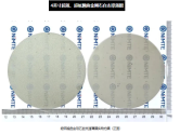
Ningbo Institute of Materials has developed a 4-inch ultra-thin, ultra-low warpage diamond self-supporting film!​

Diamond has become a key material for solving the heat dissipation problem of high-frequency and high-power chips due to its ultra-high thermal conductivity. Directly bonding chips such as silicon (Si), gallium nitride (GaN), and silicon carbide (SiC) to diamond films can significantly reduce near-junction thermal resistance and chip junction temperature, and is an ideal solution for thermal management of future high-performance chips and 3D chip packaging. Diamond films are usually nucleated and grown on substrates. However, due to the limitations of existing processes, there is a large stress between the film and the substrate and inside the film, resulting in significant warping after the substrate is removed. It is difficult to meet the warping requirements of the bonding process, which has become a core bottleneck restricting its packaging application.


1750866491017.png


In response to this challenge, the functional carbon material team led by Jiang Nan, a researcher at the Ningbo Institute of Materials Technology and Engineering, Chinese Academy of Sciences, successfully prepared a 4-inch diamond self-supporting film with a thickness of less than 100 μm through innovative technology. The self-supporting film has a warpage of less than 10 μm within a 4-inch range; it forms self-adsorption when attached to a glass substrate, fully demonstrating its ultra-high flatness and low stress characteristics . The successful development of this type of diamond self-supporting film has taken a key step in overcoming the warpage problem that has long restricted the chip bonding process and promoting the development of diamond in the field of thermal management.​

Please, Log in or Register to view URLs content!
 

gelgoog

Lieutenant General
Registered Member
So the US sanctions really worked then
They worked in that they prevented China from getting into leading edge logic. They failed in that China will dominate everything else much quicker than would have happened otherwise.

"By 2030, China is projected to dominate the global foundry landscape, accounting for 30% of installed capacity, outpacing Taiwan, South Korea, and Japan."

Mainlald China adding ~1.25 million WPM, US 375k by 2030.
Of those 375k wpm in the US only 125k wpm is in advanced nodes. The remaining 250k wpm is legacy nodes that will compete with China and much like already happened with Wolfspeed I expect it to die a slow agonizing death.

China needs to develop its own EUV tools to break the Western monopoly on leading edge logic.
 

tphuang

General
Staff member
Super Moderator
VIP Professional
Registered Member
Does anyone know the semi process and die area of 3C6000?

Please, Log in or Register to view URLs content!
Seems like 16 cores with SMT and 4-way integer per die.

I do still think they should switch to RISC-V architecture or at least cater to both RISC-V and LoongArch though.

ARM and x86 are patent minefields so it's a bad idea to use them.
I think it's still 12nm. Not sure about the die area. I think they were supposedly only moving to 7nm in 7000 series.
 

tokenanalyst

Brigadier
Registered Member

Baiao Chemical Semiconductor Base Project Starts Construction​


Xinhuilian is a semiconductor subsidiary of the listed company Bioo Chemical, and is committed to achieving the localization development of China's semiconductors and flat panel displays.

The total investment of the Xinhuilian Integrated Circuit Process Equipment R&D and Manufacturing Base project, which was laid this time, is 5 billion yuan. It will build a core equipment headquarters and R&D and production base for advanced process chip 3D integration technology.

It is reported that the R&D and manufacturing base project invested and built by Xinhuilian, a subsidiary of Baiao Chemical's semiconductor sector, officially started today. The project has a total investment of 5 billion yuan, a total construction area of about 140,000 square meters, and is expected to be completed and accepted in June 2026. After the project reaches full production, the annual output value is expected to exceed 5 billion yuan and the tax revenue will exceed 500 million yuan. It is reported that Xinhuilian is mainly engaged in the research and development and manufacturing of semiconductor wet etching, cleaning, metal stripping equipment, wafer fab automation equipment, degumming equipment, glue coating and development, wafer bonding and other equipment. Among them, the core equipment of advanced process chip 3D integration technology, wafer bonding equipment, has basically achieved domestic substitution. At present, its customers include the first-tier domestic wafer fabs and advanced packaging plants.


tokenanalyst

Brigadier
Registered Member

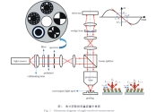
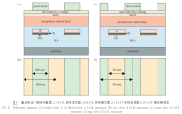
Characteristics of Aperture in Angle‑Resolved Scatterometer.​


Abstract​


With the continuous advancement of integrated circuit manufacturing technology and the reduction of device critical dimensions to nanoscale levels, high-precision overlay measurement has become a core challenge in photolithography technology. As the overlay label size gradually reduces and complex processing techniques are introduced, the aperture shape in angle-resolved scatterometer used for diffraction-based overlay (DBO) evolves from traditional annular apertures to BMW apertures and then to arch apertures, thus adapting to the constantly changing measurement needs. An optical characteristic model is constructed based on the principle of the angle-resolved scatterometer. On this basis, a simulation method for diffraction signals with different aperture shapes is proposed. The characteristics of the annular aperture, BMW aperture, and arch aperture are analyzed through theoretical analysis and simulation experiments. The performance parameter curves of overlay labels with different structural characteristics under different aperture conditions are calculated and compared. The applicable scenarios of each aperture are summarized, which provides a reference for aperture selection under various overlay label structures.

To analyze and compare the characteristics of different apertures, we propose a diffraction signal simulation method. Specifically, the shape of the converging light spot corresponding to different apertures is calculated through the Fourier transform. By sampling the pupil, we calculate the relationship between the wave vector components of the diffraction signal generated by incident light illuminating the label at various positions along the x, y, and z directions. This allows for the diffraction signal distribution at the back focal plane of the objective lens to be obtained. By combining rigorous coupled-wave analysis (RCWA), the intensity of diffraction signals at specific positions can be further calculated to determine the overlay performance parameters under different measurement conditions. The flowchart for diffraction signal distribution calculation is shown in Fig. 2. Using the proposed simulation method, the converging spot and diffraction signal distribution are simulated for different apertures, and the characteristics of each aperture are analyzed. The overlay performance parameters of conventional stacked overlay labels (Fig. 8) and multi-stacked overlay labels (Fig. 13) are simulated and analyzed under different aperture shapes and incident light parameters. Suitable scenarios for each aperture shape are provided based on the simulation results.

Based on the principle of the angle-resolved scatterometer, we propose a diffraction signal simulation method for different apertures. Using this method, the characteristics of the annular aperture, BMW aperture, and arch aperture are analyzed. Through practical simulation cases, suitable scenarios for each aperture type are presented. The research concludes that for conventional stacked overlay labels, the performance parameter curves corresponding to annular and BMW apertures are similar, with a maximum value higher than that of the arch aperture. Considering the diffraction signal characteristics of apertures, it is recommended to prioritize using BMW apertures for overlay measurements. For multi-stacked overlay labels in the preparation of 3D devices, it is recommended to prioritize using arch aperture to achieve better measurement results. The simulation method and analysis results provide theoretical support and application references for the analysis and selection of aperture characteristics in angle-resolved scatterometer.


1750955604189.png1750955634738.png

Please, Log in or Register to view URLs content!
 

tokenanalyst

Brigadier
Registered Member

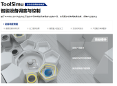
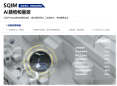
Semiconductor smart manufacturing software service provider Exxon completed hundreds of millions of yuan in financing​


Semiconductor intelligent manufacturing software service provider Exxon completed C+ financing of several hundred million yuan. This round of financing was jointly invested by Beijing Information Industry Fund and Beijing Economic Development Zone Industry Upgrading Fund managed by Jing Guorui. The funds will be mainly used to increase R&D investment, accelerate the development of new products and product iterations; expand market channels to cover more semiconductor manufacturing companies; introduce high-end talents, and improve technology and services.
Founded in 2017, Aix provides intelligent transformation technology and product services to companies in the entire semiconductor industry chain, including wafer manufacturing, equipment, packaging and testing, and materials.

1750957862187.png
1750957827652.png

Please, Log in or Register to view URLs content!
 
Top