AMEC Welcomes the Successful Delivery of the World's First Primo Menova™ 12-inch Metal Etching Equipment
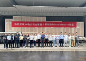
Recently, Shanghai Advanced Micro-Electronics Equipment Co., Ltd. (hereinafter referred to as "AMEC", stock code: 688012) announced that its etching equipment series has reached another milestone: the world's first Primo Menova™ 12-inch metal etching equipment has been successfully delivered to a major domestic integrated circuit R&D, design and manufacturing service provider. This milestone not only marks another independent innovation of AMEC in the field of plasma etching, but also demonstrates the company's continuous R&D technical capabilities and steady development of comprehensive strength.
AMEC's 12-inch ICP single-chamber etching equipment Primo Menova™ focuses on metal etching, especially good at etching metal Al wires and Al blocks. It can be widely used in the manufacture of power semiconductors, memory devices and advanced logic chips, and is one of the main equipment for wafer fab metallization processes. Primo Menova™ is developed and manufactured based on AMEC's mass-produced ICP etching product Primo Nanova®. It adheres to the excellent etching uniformity control and can achieve etching performance such as high rate, high selectivity and low bottom dielectric damage. Primo Menova™ is equipped with a high-efficiency chamber cleaning process to reduce chamber contamination and extend the continuous operation time of the chamber. The Primo Menova™ system also integrates a strip chamber equipped with high-temperature water vapor to efficiently remove residual photoresist and by-products on the wafer surface after metal etching. Primo Menova™ and the strip chamber can be flexibly matched according to customer process requirements to meet customers' requirements for high production efficiency to the greatest extent, ensuring the stability and yield of the machine in high-load production.
AMEC has always been at the forefront of the development of advanced process technology, moving forward in sync with the world's leading semiconductor customer companies. The company's plasma etching equipment has been used in international first-tier customers from 65 nanometers to 14 nanometers, 7 nanometers and 5 nanometers and other advanced integrated circuit processing and manufacturing production lines and advanced storage and advanced packaging production lines. The company's CCP capacitive high-energy plasma etcher and ICP inductive low-energy plasma etcher can cover more than 95% of domestic etching application needs, and meet the various stringent requirements of customers in advanced processes in terms of excellent performance and high stability. By the end of 2024, the company has accumulated more than 6,000 plasma etching and chemical thin film equipment reaction tables, and has achieved mass production and large-scale repetitive sales in 137 production lines at home and abroad.
AMEC's 12-inch ICP single-chamber etching equipment Primo Menova™ focuses on metal etching, especially good at etching metal Al wires and Al blocks. It can be widely used in the manufacture of power semiconductors, memory devices and advanced logic chips, and is one of the main equipment for wafer fab metallization processes. Primo Menova™ is developed and manufactured based on AMEC's mass-produced ICP etching product Primo Nanova®. It adheres to the excellent etching uniformity control and can achieve etching performance such as high rate, high selectivity and low bottom dielectric damage. Primo Menova™ is equipped with a high-efficiency chamber cleaning process to reduce chamber contamination and extend the continuous operation time of the chamber. The Primo Menova™ system also integrates a strip chamber equipped with high-temperature water vapor to efficiently remove residual photoresist and by-products on the wafer surface after metal etching. Primo Menova™ and the strip chamber can be flexibly matched according to customer process requirements to meet customers' requirements for high production efficiency to the greatest extent, ensuring the stability and yield of the machine in high-load production.

AMEC has always been at the forefront of the development of advanced process technology, moving forward in sync with the world's leading semiconductor customer companies. The company's plasma etching equipment has been used in international first-tier customers from 65 nanometers to 14 nanometers, 7 nanometers and 5 nanometers and other advanced integrated circuit processing and manufacturing production lines and advanced storage and advanced packaging production lines. The company's CCP capacitive high-energy plasma etcher and ICP inductive low-energy plasma etcher can cover more than 95% of domestic etching application needs, and meet the various stringent requirements of customers in advanced processes in terms of excellent performance and high stability. By the end of 2024, the company has accumulated more than 6,000 plasma etching and chemical thin film equipment reaction tables, and has achieved mass production and large-scale repetitive sales in 137 production lines at home and abroad.

