Chinese semiconductor thread II

huemens

Junior Member
Registered Member
The story about 12nm Ascend may have originated from a misinterpretation of something in a Huawei paper from June 2024. It's a paper about HiFloat8, which is a new 8-bit floating point format proposed by Huawei, that does not currently exist in any production chips. So they did all their experiments using simulation. They test how HiF8 would perform if they were added to Ascend micro-architectures referenced as XXX1 and XXX2. They also do experiments to understand extra chip area that would be needed to add HiF8 by simulating a 12nm XXX1 core using RTL code.

This doesn't necessarily mean they would use 12nm for their production chips.
But if they are really capacity constrained on 7nm then fabbing AI chips on a 12nm process and dedicating all 7nm to smartphones/laptops isn't the worst idea. AI workloads are highly parallelized and run in data-centers with abundance of power. They could get more volume of chips while adding the same amount of compute per-chip through chiplets and compensate it with more power.

Please, Log in or Register to view URLs content!

Currently, no hardware platform is available to support the HiF8 data format and complete the computation process.
This paper also evaluates the overheads and benefits of HiF8 based on the electronic system level (ESL) models of Ascend XXX1 and XXX2. When Ascend XXX1 serves as the baseline, if the computing power of HiF8 is twice that of FP16, the area of AI Core increases by approximately 4.5%, and the training performance of ResNet50 and BERT can be improved by 26% and 61%, respectively. If Ascend XXX2 serves as the baseline, the training performance of ResNet50 and BERT can be improved by 31% and 67%, respectively.
We evaluated the area overhead of HiF8 by using the register-transfer level (RTL) pilot code based on the microarchitecture of the Cube processing unit in Ascend XXX1 when K equals 32 and the chip manufacturing process is 12 nm.
 

ansy1968

Brigadier
Registered Member
Why not give us the low-down on what you know?
Sir from Motif (China military Forum)

motif
1x1.gif
pv-smile.gif


06/19/2025, 05:30:56


Please, Log in or Register to view URLs content!
|
Please, Log in or Register to view URLs content!
1x1.gif

has been completed after 8 months construction, meaning the construction started around Nov 2024, originally to be completed in Q3 this year. Yield reach 70%, use for sub-7 nm process such as the 5 nm node. Currently no official confirmation yet. If true, this means domestic 5 nm chip could be mass produced as early as end of this year, or at the latest by some time next year. Without sanction, domestic EUV couldn’t happen in mid 2025, unlikely even in 2030. With sanction, Chinese sub-5 nm chip in 2030 will be equivalent to Chinese EV today.
20250619-235242-EUV.jpg
 

tonyget

Senior Member
Registered Member
Please, Log in or Register to view URLs content!

CXMT Boosts DRAM Production by 50% in China​


China’s ChangXin Memory Technologies (CXMT) is projected to increase its DRAM shipments by 50% compared to the previous year. The company is also expected to rapidly expand its market share in the DDR5 and LPDDR5 markets, currently dominated by Korean semiconductor manufacturers such as Samsung Electronics and SK hynix.

According to Counterpoint Research’s Q1 2025 memory report released on June 20, CXMT’s production volume is expected to rise by 50% year-over-year. As a result, the company’s shipment market share in the overall DRAM market is projected to increase from 6% in Q1 to 8% in Q4.

Notably, CXMT is significantly increasing production volumes not only in its main legacy products like DDR4 and LPDDR4 but also in DDR5 and LPDDR5 products. Counterpoint forecasts that CXMT’s market share in the DDR5 market will rise from Q1 to 7% by the end of the year, and in the LPDDR5 market, it will surge from 0.5% to 9%.

The rapid increase in market share of Chinese memory companies is also evident in reports from other market research firms. According to a recent report by TrendForce, Chinese products are expected to capture a 10.1% market share in Q3 this year in terms of shipment volume in the combined DRAM and NAND memory market. This marks the first time Chinese semiconductor companies have exceeded 10% market share. After first surpassing the 5% threshold in Q2 last year with 5.4%, it has nearly doubled in just one year.

Choi Jeong-gu, principal analyst at Counterpoint, stated, “CXMT’s growth is also evident in shipments, with its market share in DDR5 and LPDDR5 markets expected to rise from less than 1% in Q1 to 7-9% in Q4.”

However, Counterpoint pointed out that CXMT is facing difficulties with the high-k metal gate process necessary for cutting-edge DRAM manufacturing. This process is an innovative technology that addresses the inevitable leakage current issues in fine processes.

Choi added, “CXMT is expected to focus on ‘3D DRAM’ innovation and continue to expand capacity. We need to pay attention to China’s growth trend.”
 

tokenanalyst

Brigadier
Registered Member

Optimizing Extreme Ultraviolet Lithography Process Metrics and Aberrations in the Cut Layer Through Source Mask Co-Optimization(SMO).​


School of Micro-Electronics, Fudan University

Abstract:​

Source-Mask Co-Optimization (SMO) techniques have significantly supported semiconductor manufacturing quality by enhancing imaging contrast and lithographic process control in advanced lithography nodes over the past decade. Through jointly optimizing the design of the illumination source and modifying the reticle patterns on the mask, the SMO techniques have provided a viable method to find the best lithography process for a given design rule. In SMO, process parameters such as the Exposure Latitude (EL), the Depth of Focus (DoF), the Mask Error Factor (MEF) can be improved through the definition of a cost function. In this presentation, we provide an example with a minimum pitch of 40 nm, which is commonly used for the 2~3 nm Back-End-Of-the-Line (BEOL) logic technology nodes. In this example, we will discuss the challenges and potential of our SMO technique and will offer recommendations for EUV SMO compensations for aberration. Our analysis indicates that SMO can continue to improve optimal pattern transfer capabilities by simultaneously optimizing both illumination source and mask design.​

Please, Log in or Register to view URLs content!
 

tokenanalyst

Brigadier
Registered Member

Array center and array corner loading effect improvement in r-SADP​


Beijing NAURA Microelectronics Equipment Co. Ltd​

Abstract:​

Reverse Self-aligned Double Patterning (r-SADP) process is a very important technique in trench etching of Dynamic Random Access Memory devices. In the r-SADP etching process, due to the distinct etching environments at the center and corner of the array, there are differences in the etched trench critical dimension at the center and corner, which will adversely affect the performance and yield of the device. This paper investigates the impact of pressure, source power, and gas during the carbon etch-back (C-EB) step in the r-SADP process on the loading effect observed at both the center and corner of the array. The results indicate that applying high pressure during the C-EB over etching step can effectively alleviate the loading effect at the center and corner of the array in the r-SADP process.​

Please, Log in or Register to view URLs content!

Etching techniques to improve the resolution pattern for DRAM
 

tphuang

General
Staff member
Super Moderator
VIP Professional
Registered Member
Please, Log in or Register to view URLs content!

CXMT Boosts DRAM Production by 50% in China​


China’s ChangXin Memory Technologies (CXMT) is projected to increase its DRAM shipments by 50% compared to the previous year. The company is also expected to rapidly expand its market share in the DDR5 and LPDDR5 markets, currently dominated by Korean semiconductor manufacturers such as Samsung Electronics and SK hynix.

According to Counterpoint Research’s Q1 2025 memory report released on June 20, CXMT’s production volume is expected to rise by 50% year-over-year. As a result, the company’s shipment market share in the overall DRAM market is projected to increase from 6% in Q1 to 8% in Q4.

Notably, CXMT is significantly increasing production volumes not only in its main legacy products like DDR4 and LPDDR4 but also in DDR5 and LPDDR5 products. Counterpoint forecasts that CXMT’s market share in the DDR5 market will rise from Q1 to 7% by the end of the year, and in the LPDDR5 market, it will surge from 0.5% to 9%.

The rapid increase in market share of Chinese memory companies is also evident in reports from other market research firms. According to a recent report by TrendForce, Chinese products are expected to capture a 10.1% market share in Q3 this year in terms of shipment volume in the combined DRAM and NAND memory market. This marks the first time Chinese semiconductor companies have exceeded 10% market share. After first surpassing the 5% threshold in Q2 last year with 5.4%, it has nearly doubled in just one year.

Choi Jeong-gu, principal analyst at Counterpoint, stated, “CXMT’s growth is also evident in shipments, with its market share in DDR5 and LPDDR5 markets expected to rise from less than 1% in Q1 to 7-9% in Q4.”

However, Counterpoint pointed out that CXMT is facing difficulties with the high-k metal gate process necessary for cutting-edge DRAM manufacturing. This process is an innovative technology that addresses the inevitable leakage current issues in fine processes.

Choi added, “CXMT is expected to focus on ‘3D DRAM’ innovation and continue to expand capacity. We need to pay attention to China’s growth trend.”
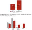
Screenshot 2025-06-20 at 10.45.14 AM.png
Here are the counterpoint diagrams.
Koreans have been saying for a few weeks now that CXMT is shifting their production to DDR5 variants. And it looks like they are really going to do that. So more DRAMs overall and bigger mix of DDR5 vs DDR4 production.
Using these projections, they could reach 9% market share in Q4 imo vs 4% in Q1
 

tokenanalyst

Brigadier
Registered Member

The Fenlianxin semiconductor core equipment project with a total investment of 1 billion yuan officially started​

According to a news release from Fenhu, on June 17, the groundbreaking ceremony for the Fenlianxin semiconductor core equipment project was held in Fenhu High-tech Zone, Suzhou City.

The project plans to invest a total of 1 billion yuan, with a land area of about 40 mu and a construction area of about 48,000 square meters. After the project is completed and put into production, it is expected to generate annual sales revenue of more than 1.5 billion yuan and annual tax revenue of more than 50 million yuan.

The project entity, Suzhou Fenlianxin Technology Co., Ltd., was established on July 17, 2024, with its registered address at No. 443, Donggang Road, Lili Town, Wujiang District, Suzhou City, Jiangsu Province, and its legal representative is Li Haiying. The business scope includes general projects: technical services, technical development, technical consulting, technical exchanges, technology transfer, technology promotion; manufacturing of special equipment for semiconductor devices; sales of special equipment for semiconductor devices, etc.

Fenhu announced that currently, Fenhu has gathered more than 50 semiconductor companies of various types, accounting for 50% of the total number of semiconductor companies in the district, basically covering the entire semiconductor industry chain including equipment materials, IC design, wafer manufacturing, packaging and testing. From January to May this year, the total industrial output value of Fenhu semiconductors and related industries increased by 17.3% year-on-year.

Please, Log in or Register to view URLs content!
 

tokenanalyst

Brigadier
Registered Member

The first phase of Guangzhou Sunyue New High-end Packaging and Testing Plant officially started.​


According to the Shanghai branch of Shaanxi Construction Sixth Construction Group, the groundbreaking ceremony for the first phase of the Guangzhou Riyue new high-end packaging and testing factory project was held on June 17.

The project has a total investment of 1.5 billion yuan and is located in the Knowledge City Semiconductor Industrial Park in Huangpu District, Guangzhou City, Guangdong Province. It has a frame structure, a construction area of 126,833.32 square meters, and a construction cost of about 320 million yuan. It aims to build a world-leading packaging and testing plant and ultimately achieve integrated circuit product packaging production capacity: 3.93 billion FCBGA/FCLGA devices/year, 230 million IGBT-SiC TO247 devices/year, 4.7 billion SOP&TSOP devices/year, 8.22 billion QFN devices/year, and 3.95 billion FCQFN devices/year.

As a key industrial project in Guangzhou, the new Riyue project covers high-end technologies such as high-precision packaging, intelligent manufacturing, and clean space. It is a landmark semiconductor packaging and testing project.

According to information, Guangzhou Riyuexin was established in September 2022 with a registered capital of US$100 million. It specializes in the design, manufacturing and sales of integrated circuit chips.

Please, Log in or Register to view URLs content!
 
Top