Chinese semiconductor thread II

tokenanalyst

Brigadier
Registered Member

Huacan Optoelectronics GaN is fully connected, focusing on 4 major areas​


● In terms of gallium nitride devices , BOE Huacan Optoelectronics started in the consumer electronics market and gradually moved towards the medium and high-power power electronics markets such as data centers and industrial vehicles. In this regard, BOE Huacan Optoelectronics has developed a variety of 650V series products. The reserve product voltage is as high as 1200V , covering different power ranges, with a variety of packaging methods, which can match different scenarios such as mobile phone fast charging, computer adapters, and server power supplies. need.

● In terms of self- produced epitaxial wafers , the GaN epitaxial wafers exhibited this time have reached the ideal production level with corresponding device yields. Self-produced GaN epitaxial wafers can achieve better device results and performance parameters. BOE Huacan Optoelectronics has achieved optimization of crack-free HEMT epitaxy on 6/8-inch silicon substrates , and the surface roughness and thickness consistency have reached ideal levels. According to test verification, BOE Huacan Optoelectronics’ GaN epitaxy’s static parameters such as threshold voltage, withstand voltage, gate voltage tolerance, etc. can benchmark against domestic and foreign leading products.

● In terms of its own process lines , BOE Huacan Optoelectronics has a GaN production line, which will be fully operational in 2023 and can realize tape-out from epitaxy to chip. It is expected to achieve an annual production capacity of 12,000 devices in 2024.

● Our own substrate factory, Blue Crystal Technology, has achieved specification optimization and mass production of 6 -inch sapphire substrates, and has also begun product reserves of 8-inch sapphire substrates, which can self- produce high-voltage, cost-effective GaN on sapphire devices in the future. Products pave the way.
 

tokenanalyst

Brigadier
Registered Member

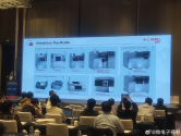
Thermal NIL PRO: The next stage in the high-volume production of nanodevices

Massimo Tormen from Qingdao Tenren Micro-Nano gave a report titled "Thermal NIL PRO: The next stage in the high-volume production of nanodevices".
Nanoimprinting is a technique for replicating structures with nanoscale precision. It has been named one of the "top ten emerging technologies that will change the world" by MIT Weekly. After more than 20 years of development, basic research on nanoimprint technology has matured, and substantial progress has been made in equipment, molds, materials and processes. With the promotion of micro-nano structures in products, the advantages and importance of nanoimprinting have attracted more and more attention. Qingdao Tenren Micro-Nano nanoimprint technology provides a complete solution for nanolithography, with a precision better than 50 nanometers and an aspect ratio of 10:1 in a 12-inch area, which can be widely used in the production of micro-nano structure products.

1705091838495.png
 

european_guy

Junior Member
Registered Member

Tech war: China chip imports fall in 2023 but semiconductors remain country’s largest item ahead of crude oil​


Please, Log in or Register to view URLs content!

In 2023, China imported a total of 479.5 billion IC units worth US$349.4 billion, down 10.8 per cent by volume and 15.4 per cent in value from 2022, official data showed.

...this drop in import will never be recovered, it is a deep structural change that is ongoing in China semiconductor market: localization is the new rule.

According to the customs data, China’s imports of diodes and similar semiconductor devices, a proxy of garden-variety commodity chips, were also down by 23.8 per cent in volume terms last year.

...and this is just the beginning...

China currently has 44 semiconductor wafer fabs in operation and a further 22 under construction, Taiwan-based IC research company TrendForce said in a recent note. By the end of 2024, the capacity for mature chip production – defined as 28-nanometre and older technologies – will be expanded at 32 Chinese fabs.

If the planned fab expansion will go smoothly (of course US will do its best to hamper it), then the drop in IC import will be even bigger.
 

tokenanalyst

Brigadier
Registered Member

AMEC: Net profit is expected to increase by approximately 45% to 58% year-on-year in 2023​

China Microwave Corporation recently released its annual performance forecast, predicting operating revenue of approximately 6.26 billion yuan in 2023, an increase of approximately 1.52 billion yuan compared with 2022, and a year-on-year increase of approximately 32.1%. The value of new orders in 2023 will be approximately 8.36 billion yuan, an increase of approximately 2.04 billion yuan compared with 2022, and a year-on-year increase of approximately 32.3%.
According to the announcement, the company's main equipment products, CCP and ICP plasma etching equipment for integrated circuit production lines, are expected to have operating revenue of approximately 4.70 billion yuan in 2023, an increase of approximately 1.56 billion yuan from 2022, and a year-on-year increase of approximately 49.4%. The value of new etching equipment orders in 2023 will be approximately 6.95 billion yuan, an increase of approximately 2.61 billion yuan compared with 2022, and a year-on-year increase of approximately 60.1%.
The company expects to achieve a net profit attributable to the owners of the parent company of 1.70 billion yuan to 1.850 billion yuan in 2023, which will increase by 530 million yuan to 680 million yuan compared with the same period last year (statutory disclosure data), a year-on-year increase of approximately 45.32% to 58.15%.

Please, Log in or Register to view URLs content!
 

tokenanalyst

Brigadier
Registered Member

Guangsiao’s new pan-semiconductor manufacturing high-end technology and automation equipment base​


the groundbreaking ceremony of the Guangsi Aofan Semiconductor high-end process and automation equipment production base project was held - it is a special honor to invite everyone present to witness this important moment.

Suzhou Guangsiao Optoelectronics Technology Co., Ltd. is a high-tech enterprise integrating R&D, manufacturing, sales and after-sales. Mainly for the semiconductor, FPD and new energy industries, it provides process equipment, non-standard equipment customization, software and hardware transformation services, with the goal of breaking international monopoly, realizing the localization of high-end equipment, and providing customers with high-efficiency, low-cost and optimized overall solutions. plan, committed to becoming a leader in the field of advanced manufacturing of Chinese equipment.

Please, Log in or Register to view URLs content!
 

tokenanalyst

Brigadier
Registered Member

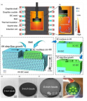
New breakthrough in wafer-level cubic silicon carbide single crystal growth!​


Silicon carbide (SiC) has excellent properties such as wide bandgap, high breakdown field strength, high saturation electron drift rate and high thermal conductivity, and has important applications in fields such as new energy vehicles, photovoltaics and 5G communications. Compared with 4H-SiC, which is currently widely used, cubic SiC (3C-SiC) has higher carrier mobility (2-4 times), low interface defect state density (1 order of magnitude lower) and high electron density. Affinity (3.7 eV). Using 3C-SiC to prepare field-effect transistors can solve problems such as poor device reliability caused by many gate-oxide interface defects. However, 3C-SiC-based transistors have made slow progress, mainly due to the lack of single crystal substrates. A large number of previous studies have shown that 3C-SiC is prone to phase changes during the growth process, and existing growth methods cannot obtain single crystal forms.

According to the classical crystal growth theory, for smooth interface crystals, homogeneous two-dimensional nucleation needs to overcome a critical barrier, there is a critical Gibbs free energy or supersaturation, and growth can proceed at an arbitrarily small supersaturation. For heterogeneous nucleation, due to the introduction of new solid-solid interface energy, two-dimensional nucleation needs to overcome a higher critical barrier. Therefore, under the same supersaturation, homogeneous nucleation and growth are energetically significantly better than heterogeneous nucleation and growth, making the latter difficult to occur.

Recently, Chen Xiaolong's team from the Institute of Physics, Chinese Academy of Sciences/Beijing National Research Center for Condensed Matter Physics proposed the academic idea of regulating the solid-liquid interface energy to nucleate and grow on heterogeneous seed crystals preferentially over homogeneous seed crystals. Mainly including: 1) The lattice mismatch between the 3C (111) plane and the 4H (0001) plane is small, and the solid-solid interface energy is very low; 2) The difference in Gibbs free energy between 4H and 3C bulk phases is small; 3) If By controlling the melt composition, the interface energy of 3C(111)-melt is sufficiently lower than that of 4H(0001)-melt. The Gibbs free energy of two-dimensional nucleation and subsequent growth is more beneficial to the 3C phase. The team independently designed and built ultra-high temperature melt surface tension and solid-liquid contact angle testing equipment, measured the surface tension of melts with different components at high temperatures, and the contact angles between the melt and 4H-SiC and 3C-SiC, and obtained The changing rules of the solid-liquid interfacial energy of 4H-SiC, 3C-SiC and high-temperature melts were studied, and the feasibility of interfacial energy regulation was verified. The team used the high-temperature liquid phase method to achieve the requirement of lower Gibbs free energy of 3C-SiC under the same supersaturation condition, suppressing the phase transition during the growth process, and grew a 2-4 inch diameter cell for the first time in the world. 3C-SiC single crystal with a thickness of 4-10mm and a single crystal form, as shown in Figures 1 and 2.

1705244986074.png

Please, Log in or Register to view URLs content!
 

Weaasel

Senior Member
Registered Member
New Thread? It's been a while since I have been here... I must say the Chinese Semiconductor Industry Thread and the Carl Zeiss thread before it that started that one, were all very informative and educational.

And you know what we have to thank for starting all that?

Many of you are not going to like it...

TIDALWAVE ...
 

Wrought

Junior Member
Registered Member
Seems that small quantities of A100/H100 chips are still circulating publically in 2023. One wonders how much is not made public.

Buying or selling high-end U.S. chips is not illegal in China and the publicly available tender documents show dozens of Chinese entities have bought and taken receipt of Nvidia semiconductors since restrictions were imposed.

Please, Log in or Register to view URLs content!
 
Top