Chinese semiconductor thread II

tokenanalyst

Brigadier
Registered Member

Research on High-Precision Position Detection Based on a Driven Laser Spot in an Extreme Ultraviolet Light Source​

State Key Laboratory of Laser Interaction with Matter, Changchun Institute of Optics, Fine Mechanics and Physics, Chinese Academy of Sciences, Changchun 130033, China
University of Chinese Academy of Sciences, Beijing 100049, China

Abstract​

Laser-spot-location detection technology based on photodetectors is widely used in the aerospace, medical, military and communication fields. However, most of the current research focuses on continuous laser detection in the visible and near-infrared bands, and the real-time high-precision position detection of a long-wave infrared pulsed laser is lacking. In this paper, a spot-position detection system based on a four-quadrant detector is designed for a 10.6 μm CO2-driven laser in extreme ultraviolet light source, and a second-order extended error compensation algorithm based on a Gaussian-spot model is proposed. Finally, the algorithm is verified and analyzed experimentally by a spot-position detection system under both focusing and defocusing conditions. The experimental results show that the root-mean-square error, maximum absolute error and average absolute error of the second-order error compensation algorithm are significantly reduced compared with the traditional algorithm, and the detection accuracy of the spot-position is better than 9 μm. The above results show that this spot-position detection system has obvious advantages and high accuracy, which can realize the high-precision real-time detection of a laser’s spot position to obtain accurate spot position information, provide feedback adjustments for subsequent beam pointing control, and provide a theoretical basis for the beam pointing stability of the extreme ultraviolet light source system.​

View attachment 123957

Please, Log in or Register to view URLs content!
 

tokenanalyst

Brigadier
Registered Member

Research on Ultra-Precision Displacement Measurement Technology Based on Single-Path Littrow Grating Interferometer​


Institute of Precision Optical Engineering, Tongji University, Shanghai 200092, China
MOE Key Laboratory of Advanced Micro-Structured Materials, Tongji University, Shanghai 200092, China
Shanghai Frontiers Science Center of Digital Optics, Tongji University, Shanghai 200092, China.
Shanghai Professional Technical Service Platform for Full-Spectrum and High-Performance Optical Thin Film Devices and Applications, Tongji University, Shanghai 200092, China
School of Physics Science and Engineering, Tongji University, Shanghai 200092, China
College of Metrology and Testing Engineering, China Jiliang University, Hangzhou 310018, China


Abstract: Ultra-precision displacement measurement technology based on grating interferometer is a key common technology in the field of advanced manufacturing. Using gratings with higher density of lines is an effective way to improve the measurement accuracy and resolution of grating interferometer. With the improvement of electron beam preparation grating technology, the use of electron beam processing high-line density grating (more than 3000 lines/mm) as the measurement benchmark is an effective way to optimize the performance of the interferometer. Using a high line density electron beam direct writing grating of 3333 lines/mm and a single-channel Littrow grating interference configuration, a grating interferometer with an original signal period of 300 nm was built, which verified its accuracy and accuracy in displacement measurement. stability. The single-channel Littrow grating interferometer and laser interferometer comparison device provides new possibilities for subsequent grating spacing calibration, and is a useful exploration of electron beam direct writing high-line density gratings in the field of precision displacement measurement.

Please, Log in or Register to view URLs content!
 

gelgoog

Lieutenant General
Registered Member
"China’s chipmaking capacity will more than double in five to seven years based on local manufacturers’ existing plans, “materially more” than the market expects, according to research from Barclays analysts."
Yeah. Assuming the Chinese fab expansion plans are achieved.

"Most of that additional production capacity could be added in the next three years, based on an analysis of 48 chipmakers with fabrication plants in mainland China, the research showed.

“Local players are still underappreciated,” analysts including Joseph Zhou and Simon Coles said in the note on Thursday. “There are materially more local semiconductor manufacturers and fabs in China than suggested by mainstream industry sources.”"
Of course. If you read mainstream Western publications you would think that SMIC and YMTC are the only players. Maybe CXMT. But companies like Hua Hong, Nexchip, CanSemi, GTA Semiconductor are basically not mentioned.

"China is working toward technological self-sufficiency, something that’s become more difficult after the US and some of its allies restricted what tech companies were allowed to sell into the Asian country. Chinese firms have accelerated purchases of vital chipmaking tools to support the ramp-up and to build supplies ahead of new bans."
It is because of the US bans that the Chinese chip industry was kicked into overdrive. If we were relying just on Chinese government directives this might have taken 3x as long to happen. SMIC for example might have been building a small highly expensive EUV fab to make 5nm. Instead they spend the same amount of money on a gargantuan amount of 28nm output. Like 4x the wafers that EUV fab would have produced or more.

"Leading chip gear producers, including the Netherlands’ ASML Holding NV and Japan’s Tokyo Electron Ltd., saw an inrush of orders from China last year."
The Japanese even made a new fab to make lithography tools. Do you think it was made to supply Japanese clients or US clients or whatever? Clearly aimed at the Chinese market.

"Most of the additional capacity will go to producing chips using older technology, the analysts said. These legacy semiconductors — at 28 nanometers and above — are at least a decade behind the most advanced chips, but are widely used in systems such as home appliances and automobiles."
With these fabs even if China gets cut out of Western chips altogether they will be able to retain a XXIst century lifestyle level in perpetuity. And it is highly unlikely leading edge fabs will be ever competitive with legacy nodes for those applications. The cost per transistor keeps increasing with more modern processes.

"These chips could theoretically cause an over-supply in the market, the Barclays analysts said, though “we see this as at least some years away, likely 2026 at the earliest, and dependent on the quality achieved as well as any new trade restrictions.”"
The thing is it is not just China that is building fabs for legacy nodes. The same thing is happening in the US, Japan, and the EU. But you don't see people talking about hat.

"China’s ambition in legacy semiconductors has drawn attention from the US Commerce Department, which plans to gather information on how deeply reliant US firms have become on the technology from China. Bloomberg News reported in December that the US could impose tariffs or other trade restrictions to counter China’s push."
Of course they will impose tariffs. And guess what the Chinese will continue to export their consumer appliances all over the rest of the world which is a much larger market than the US.

"China currently controls about 30% of manufacturing capacity globally for 50-180nm chips that are commonly used in power switches, internet-of-things (IoT) devices and sensors. The figure is expected to grow to 35% within the next five years and 46% within a decade.

TrendForce, a Taipei-based market intelligence provider, said in a report last October that only about 30% of the global production capacity will be used to make advanced chips below 16nm by 2027 while the remaining 70% will still be used to make chips above 28nm."
30% by what? Value? Area? Number of ICs?

"It said China’s share in global mature process capacity is anticipated to grow from 29% in 2023 to 33% in 2027 while Taiwan’s share will fall from 49% to 42%. Major players in China include Semiconductor Manufacturing International Corp (SMIC), HuaHong Group and Nexchip."
If doubt it will just go from 29% to 33%. Just look at SMIC's planned expansion. Gargantuan in nature. Nexchip went from basically nothing to being in the top 5 foundries. And Hua Hong is also massively expanding legacy node capacity.
 
Last edited:

tokenanalyst

Brigadier
Registered Member

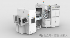
Warm congratulations to Yuan Lei Nano on the shipment of its first advanced process ALD cluster machine​


On January 13, 2024, the first advanced process ALD cluster machine A300 independently developed by Yuanlei Nano was successfully delivered to customers. This progress not only reflects Yuanlei Nano’s innovative strength in the field of ALD advanced process equipment, but also demonstrates Yuan Lei Nano’s firm determination and remarkable achievements in promoting the localization of the semiconductor industry. This innovative achievement of Yuanlei Nano has injected new vitality into the development of China's integrated circuit industry.

The ALD cluster equipment A300 shipped by Yuanlei Nano this time is a key thin film deposition equipment for advanced integrated circuit processes . It is based on the Elegant Cluster platform independently developed by Yuanlei Nano . It is mainly used in logic and storage devices of 12 -inch advanced processes. Production and manufacturing to meet various film deposition needs of oxides, nitrides, metals, etc. Cluster A300 realizes the seamless connection between PE and Thermal processes, greatly improving process stability and production efficiency. Among them, the Thermal ALD process chamber is equipped with a plasma self-cleaning function, which helps to improve the reliability of the equipment and extend the PM cycle, further improving the performance and competitiveness of Cluster A300. The platform's various process performances have reached the international advanced level and have been recognized by many customers.

1705415832594.png

Since its establishment, Yuanlei Nano has deeply cultivated ALD equipment technology. Through continuous innovation and breakthroughs, the product line has achieved comprehensive coverage in the fields of advanced integrated circuit processes, compound semiconductors , optoelectronics, new energy, optics, scientific research, etc., filling a number of Localization is blank.Adhering to the core values of " professionalism, innovation, integrity, and responsibility " , Yuanlei Nano continues to pursue excellence, innovative development, and makes unremitting efforts to build a high-end national brand of purely domestically produced advanced semiconductor equipment .​


Please, Log in or Register to view URLs content!
 
Last edited:

tokenanalyst

Brigadier
Registered Member

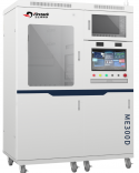
Hangzhou Feiste Technology SiC testing equipment was successfully certified as the first equipment (set) in Zhejiang Province​


On January 15, Hangzhou Feiste Technology Co., Ltd. (hereinafter referred to as "Feiste") issued an official Weibo statement stating that the company's SiC device intelligent dynamic testing equipment was successfully selected and recognized as the first equipment (set) in Zhejiang Province.

According to reports, the SiC device intelligent dynamic test equipment is a power semiconductor dynamic parameter test system developed by Feiste based on more than 10 years of experience in SiC MOSFET/IGBT applications. It has experienced three generations of product iterations: ME100D, ME200D, and ME300D. The test voltage can reach up to 6000V. , current 10000A, parasitic inductance <10nH.

At present, this series of equipment has been used in State Grid, SAIC, FAW, BYD, Geely, NIO, Inovance Technology, CATL, Great Wall, Infineon, Mitsubishi Electric, CRRC Semiconductor, Silan Microelectronics, Shanghai Aerospace, Special It has been applied by enterprises, universities, and scientific research institutions such as electrical substations, Zhejiang University, and Fudan University, and has received high praise from customers.

1705416631130.png

According to Feiste's official website, the company focuses on the application of power semiconductors such as IGBT and SiC MOSFET, and specializes in the research, development and sales of power system core components and power semiconductor testing equipment.

In addition to the above equipment, its testing equipment related to SiC MOSFETs also includes dynamic and static ATE testing equipment for new power device production lines and dynamic characteristic testing equipment in the laboratory.​

Please, Log in or Register to view URLs content!
 

sunnymaxi

Captain
Registered Member
Chinese scientists have proposed a new quantum sensing paradigm to provide technical support for defect detection of chips below ten nanometers..

Introduction: Recently, Chinese scientists have made important progress in the field of quantum precision measurement, proposing a new quantum sensing paradigm based on signal correlation, achieving high-precision imaging of point defects in diamond, and observing the charge dynamics of point defects in real time.

Recently, Academician Du Jiangfeng, Professor Wang Ya and others from the Key Laboratory of Microscopic Magnetic Resonance of the Chinese Academy of Sciences at the University of Science and Technology of China have made important progress in the field of quantum precision measurement. They proposed a new quantum sensing paradigm based on signal correlation to achieve high detection of point defects in diamond. Precision imaging, and the charge dynamics of point defects were observed in real time. Relevant research results were recently published online in "Nature Photonics".

In this work, the research team proposed a new quantum sensing paradigm, which uses the signal correlation between multiple quantum sensors to improve the analysis capabilities and reconstruction accuracy of complex objects. Based on the independently developed nitrogen-vacancy color center preparation technology, the research team can controllably prepare three nitrogen-vacancy color centers about 200 nanometers apart as a quantum sensing system. They demonstrated this new quantum sensing by detecting random electric fields. paradigm.

Diamond is a wide-bandgap semiconductor material with excellent properties. The charge dynamics of point defects in the material will bring random electric field noise. The research team successfully located 16 point defects within the micron range, with a maximum positioning accuracy of 1.7 nanometers. Based on this ability of correlation resolution and precise positioning, they also achieved in-situ real-time detection of the charge dynamics of each point defect, providing a new method for studying the properties of point defects within bulk materials. According to the researchers, this achievement demonstrates ultra-high sensitivity defect detection based on quantum technology, which can detect even one defect in one hundred billion normal atoms. This is more than two orders of magnitude higher than the detection limit of the current most sensitive method, and is expected to provide a powerful technical means for defect detection in current chips below ten nanometers.

Please, Log in or Register to view URLs content!
 

tokenanalyst

Brigadier
Registered Member

Semiconductor advanced packaging technology company Xind Semiconductor received 600 million yuan in strategic financing, led by Kunqiao Capital and Shanghai National Policy​


Recently, Xind Semiconductor, a semiconductor advanced packaging technology company, completed a strategic financing of 600 million yuan. This round of financing was led by Kunqiao Capital and Shanghai National Policy, and was followed by Weilan Venture Capital, Ningbo Yushan, Zhuoyuan Capital, Longcheer and others.

It is understood that this round of financing will further expand and consolidate the development of the advanced packaging and testing industry.

Jiangsu Xinde Technology Semiconductor Technology Co., Ltd. was established in September 2020. It is mainly engaged in integrated circuit packaging and testing business. Its main business includes the development of integrated circuit packaging and testing solutions, packaging processing of different types of integrated circuit chips and finished product testing services.

Since the establishment of the company, Core Semiconductor has actively deployed in the field of advanced packaging and testing, formed a rich reserve of packaging technology, and is committed to the research, development and production of the world's leading packaging and testing technology to create a world-leading packaging and testing enterprise. Its products mainly include Products in packaging forms such as QFN, WLCSP, BGA, LGA, SiP, WLCSP, POP, FANOUT and 2.5D/3D, and have outstanding process advantages and technological advancement in key areas of advanced packaging such as bumping and FC.​

Please, Log in or Register to view URLs content!
 

tokenanalyst

Brigadier
Registered Member

China Electronics Technology's high-end semiconductor equipment development accelerates​

At the beginning of the new year, China Electronics Technology Co., Ltd. independently developed high-end semiconductor equipment such as SiC epitaxial furnaces, laser sealing and welding equipment, HP-6100 automatic dicing machines, etc., to start an intensive delivery mode, leading the maintenance with hard work and innovation.

At the beginning of the new year, CETC's independently developed high-end semiconductor equipment such as SiC epitaxial furnaces, laser sealing and welding equipment, and HP-6100 automatic dicing machines have started an intensive "delivery mode" to ensure high-quality development through practical innovation and leadership.

40 independently developed SiC epitaxial furnaces have been successfully installed at the customer's site, and the technical team is speeding up the installation and debugging work to ensure equipment delivery and acceptance. SiC is an ideal material for making high-temperature, high-frequency, and high-power electronic devices. There is an increasing demand for applications in new energy vehicles, photovoltaic industry, high-voltage transmission and distribution lines, and smart power stations. SiC epitaxial equipment, as one of the core equipment for manufacturing third-generation semiconductor SiC devices, is extremely difficult to develop and plays an important role in the entire industry chain. At present, more than 100 SiC epitaxial furnaces have been successfully shipped, and the stable equipment performance continues to receive multiple market orders and customer praise.

The self-developed laser sealing and welding equipment was successfully shipped to the customer site. This is the first equipment shipped this year and the 50th equipment shipped in total, and is well received by users. Laser sealing and welding equipment is a key equipment in the manufacturing of microwave components. It is mainly used for air-tight packaging of components. It can effectively protect the internal bare chips and circuits from the external environment and ensure the long-term reliability and stability of component performance. The equipment has maintained a leading position in the domestic market share all year round, effectively ensuring the innovative development in the field of micro-assembly.

Dozens of independently developed HP-6100 automatic dicing machines are shipped to customer sites in batches. The dicing machine is an important equipment in the semiconductor packaging process. The HP-6100 automatic dicing machine is widely used for cutting a variety of materials, especially for multi-piece cutting. It is suitable for ceramic substrates, glass, packages, silicon wafers, etc. The dicing process of discrete devices is a "star model" among dicing products that has been polished and cultivated for many years. The scientific research team is accelerating technological research and update iterations, contributing to the realization of high-level scientific and technological self-reliance and self-reliance.


Please, Log in or Register to view URLs content!
 

tokenanalyst

Brigadier
Registered Member

Micron Corporation (AMEC): Revenue continues to grow at a high rate and etching orders grow significantly​

 
 The company expects full-year operating income in 2023 to be 6.26 billion yuan, +32.1% year-on-year. The company's average annual revenue growth rate exceeded 35% over the past ten years from 2012 to 2023, achieving sustained, stable and high growth; from an order perspective, the company's new annual revenue in 2023 The number of signed orders was 8.36 billion yuan, a year-on-year increase of 32.3% compared to the 6.32 billion yuan in new orders signed in 2022, ensuring continued high growth in performance in 2024.

  Etching equipment: Benefiting from the company's complete layout of single and dual etching equipment, continuous breakthroughs in core technology, rapid iteration of product upgrades, and rich etching application coverage, the company's CCP and ICP etching equipment will be among the leading domestic manufacturers in 2023. The market share of customer chip production lines has increased significantly; the company's TSV through-silicon via etching equipment is also increasingly used in advanced packaging and MEMS device production; the annual revenue in 2023 is expected to be 4.7 billion yuan, +49.4% year-on-year, new Increased orders were 6.95 billion yuan, +60.1% year-on-year.

Transform to a platform and continue to be optimistic about the breakthrough of new equipment to open up the growth ceiling.

  The company has gradually transformed from deep etching to a platform enterprise, and has steadily promoted new product development and industrialization. The progress is gratifying:

1) Four new equipment products have been newly developed in the past two years, including LPCVD and ALD, which have entered the market. Three pieces of equipment have been certified by customers and have begun to receive repeated orders;

2) The company's newly developed silicon and silicon germanium epitaxial EPI equipment, wafer edge Bevel etching equipment and other new products will also be put into market verification in the near future;

3) The company has also made good progress in developing various types of MOCVD equipment required for silicon carbide power devices, gallium nitride power devices, Micro-LED and other devices, and will gradually enter the market in 2024
. Looking forward to the future, we are optimistic about the company's layout and breakthroughs in new products and opening up the growth ceiling.
 
Top