Chinese semiconductor thread II

sunnymaxi

Major
Registered Member
A few articles I found.

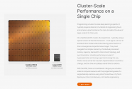
Firstly, a wafer sized "big chip" for AI applications. Is this viable?

Please, Log in or Register to view URLs content!

China poaching Koran DRAM workers:

Please, Log in or Register to view URLs content!

Naura tools surge:

Please, Log in or Register to view URLs content!
NAURA/AMEC annual report include orders already posted by @tokenanalyst ...

a wafer sized "big chip" for AI applications this news also posted by @tokenanalyst

AMEC tools order and annual report. just posted above your post..

Micron Corporation (AMEC): Revenue continues to grow at a high rate and etching orders grow significantly​

 
 The company expects full-year operating income in 2023 to be 6.26 billion yuan, +32.1% year-on-year. The company's average annual revenue growth rate exceeded 35% over the past ten years from 2012 to 2023, achieving sustained, stable and high growth; from an order perspective, the company's new annual revenue in 2023 The number of signed orders was 8.36 billion yuan, a year-on-year increase of 32.3% compared to the 6.32 billion yuan in new orders signed in 2022, ensuring continued high growth in performance in 2024.

  Etching equipment: Benefiting from the company's complete layout of single and dual etching equipment, continuous breakthroughs in core technology, rapid iteration of product upgrades, and rich etching application coverage, the company's CCP and ICP etching equipment will be among the leading domestic manufacturers in 2023. The market share of customer chip production lines has increased significantly; the company's TSV through-silicon via etching equipment is also increasingly used in advanced packaging and MEMS device production; the annual revenue in 2023 is expected to be 4.7 billion yuan, +49.4% year-on-year, new Increased orders were 6.95 billion yuan, +60.1% year-on-year.

Transform to a platform and continue to be optimistic about the breakthrough of new equipment to open up the growth ceiling.

  The company has gradually transformed from deep etching to a platform enterprise, and has steadily promoted new product development and industrialization. The progress is gratifying:

1) Four new equipment products have been newly developed in the past two years, including LPCVD and ALD, which have entered the market. Three pieces of equipment have been certified by customers and have begun to receive repeated orders;

2) The company's newly developed silicon and silicon germanium epitaxial EPI equipment, wafer edge Bevel etching equipment and other new products will also be put into market verification in the near future;

3) The company has also made good progress in developing various types of MOCVD equipment required for silicon carbide power devices, gallium nitride power devices, Micro-LED and other devices, and will gradually enter the market in 2024
. Looking forward to the future, we are optimistic about the company's layout and breakthroughs in new products and opening up the growth ceiling.
 

sunnymaxi

Major
Registered Member
Not to mention that work environment in SK is probably most toxic in the more, more so than Taiwan, Japan, or mainland China. A lot of them are looking to get out of the country asap.
very few people know this ..

A large number of Japanese scientists/engineers currently working in Chinese mainland labs.. same with Koreans/Taiwanese in semiconductor and display industries.. China is suitable for them. similarity in culture and society. best wages with low inflation rate and very near to homeland. so easy to travel.

Japanese researchers openly admitted, China currently have best laboratories for research. equipped with world class instruments. ''we were looking for independent lab for research in Japan but failed to secure funding, we moved to mainland China and immediately got approval to open laboratory''.. A reputed Japanese scholar..
 
Last edited:

antiterror13

Brigadier
Please, Log in or Register to view URLs content!

There's been some hubbub about SK Hynix upgrading its Wuxi plant and working around the sanctions on EUV. It's been speculated that they do part of the process in Wuxi, then ship the wafers to the Incheon plant for the EUV step and transporting them back to Wuxi for the rest.

Thats too complicated and costly, too many potential failures
 

BoraTas

Captain
Registered Member
Not to mention that work environment in SK is probably most toxic in the world, more so than Taiwan, Japan, or mainland China. A lot of them are looking to get out of the country asap.
Taiwanese and South Koreans are working themselves to burnout. There are no ways you could have Westerners work for that many hours and accept getting disrespected by their superiors that commonly.
Firstly, a wafer sized "big chip" for AI applications. Is this viable?
Yes. In fact such chips are particularly advantageous in many HPC and AI applications. Supercomputing clusters waste a lot of energy and time sending data between the memory and the processor, between memory banks (such as from a card's memory to another card's memory) and between nodes. Nvidia's NVLink was very important because of this and it is one of the reasons why Nvidia did so well against AMD and Intel in AI accelerator business. With a wafer scale chip, you have much less nodes and the nodes have a single processor and a single memory bank. Also all of the said hardware are on a single die. These make handling of data much faster (incomparably) and efficient.

WSE-2.png
There is a reason they advertise data handling metrics. The difference is beyond comparison. Simply different universes

I must say this graph is a bit manipulative (it is not very clear what they mean by fabric bandwidth and the number of cores is a meaningless metric on its own) but it shows the difference in data handling very well.
 
Top