It’s actually become like this for the ASICs market too though I don’t remember which companies are dominating the platform standards (not China to my knowledge but maybe there are domestic players in here now).yeah, I hadn't followed this space before, but was shocked today to hear just how dominant they are in the space they are in. Apparently, anyone doing electronics have to learn to use the dev kits. That's a pretty good moat to have.
Especially since all the consumer IoT devices are produced in China these days.
I just wish more Chinese chip designers actually take advantage of the huge market they have.
Rockchip is kind of doing that in the SBC space, but honestly, their chips are not that good. They just got such a huge head start that the entire software/dev ecosystem is on their side.
You are using an out of date browser. It may not display this or other websites correctly.
You should upgrade or use an alternative browser.
You should upgrade or use an alternative browser.
Chinese semiconductor thread II
- Thread starter vincent
- Start date
Fuga Gallium Industry successfully developed gallium oxide MOCVD homoepitaxial wafer
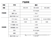
Recently, Hangzhou Fuga Gallium Technology Co., Ltd. (hereinafter referred to as Fuga Gallium) has made another breakthrough in gallium oxide MOCVD homoepitaxial technology. Tests by the national authoritative testing agency, the China Institute of Metrology, show that the carrier concentration of gallium oxide homoepitaxial wafers with a thickness of more than 10μm is 4.2E16 cm -3 , and the mobility reaches 181.6 cm2 / V·s. The successful development of high-quality gallium oxide homoepitaxial wafers based on MOCVD technology will effectively help the rapid implementation of the gallium oxide high-voltage and high-power power electronic device industry.
Major breakthrough! The first domestically produced photonic chip has achieved mass production, from Wuxi!
According to the latest news from the Wuxi Photonic Chip Research Institute of Shanghai Jiao Tong University, at 4 pm on June 5, the Wuxi Photonic Quantum Chip Pilot Platform successfully rolled off the first 6-inch thin-film lithium niobate photonic chip wafer . This is China's first photonic chip pilot line. At the same time, high-performance thin-film lithium niobate modulator chips with ultra-low loss and ultra-high bandwidth have also been mass-produced.
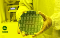
he 6-inch wafer produced by the Wuxi platform is a major breakthrough in the preparation of domestic photonic quantum chip materials . Large-size wafers directly determine the number of chips that can be obtained in a single tape-out, and are a key springboard for cost control and large-scale production. Through independent innovation, the platform has achieved major breakthroughs in film stripping, wafer bonding, nano-level precision processing and other links, laying a solid foundation for subsequent chip design, tape-out, packaging and testing.
According to the person in charge of the Wuxi Photonic Quantum Chip Pilot Plant, "A 6-inch diameter wafer can be cut into 350 chips . After the test reaches full production, the Wuxi Photonic Quantum Chip Pilot Plant will have the capacity to mass produce 12,000 thin-film lithium niobate wafers per year ."
At the same time, photonic quantum chips are the core hardware carrier of photonic quantum computing . Their industrialization process will promote China's independent control in the field of quantum information, and it is also a strategic support for seizing the commanding heights of global quantum technology competition.
The successful preparation of thin-film lithium niobate chip wafers has far more significance than the material itself . When photonic quantum chips are widely used in optical communications, quantum computing, precision sensing and other fields, a new information processing paradigm will be opened up - photonic quantum computing is expected to solve complex problems that are difficult for classical computers to solve, high-speed optical communications will redefine the boundaries of network bandwidth, and high-precision quantum sensing may revolutionize medical imaging and environmental monitoring technologies .
NAURA PVD equipment shipments exceeded 1,000 units
NAURA held a grand ceremony to celebrate the delivery of the 1,000th PVD complete machine. This is the third milestone in the company's product category that has exceeded 1,000 units in shipments, following etching equipment and vertical furnace equipment.
PVD ( physical vapor deposition ) technology is a key link in chip manufacturing, especially in the preparation of metal films.
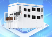
NAURA has been deeply engaged in the research and development of PVD equipment since 2008. The company has successfully launched more than 40 mass-produced PVD equipment, with cumulative shipments reaching 1,000 units and more than 5,000 chambers, and has become a leading domestic PVD equipment solution provider. Its products are widely used in semiconductor and pan-semiconductor fields such as logic, storage, power devices, advanced packaging, silicon-based micro-displays, MEMS (micro-electromechanical systems), semiconductor lighting, etc., providing solid support for industrial development.
World class 12bit 16GSPS 4-channel ADC unveiled. ADC is the crucial IC part in AESA radars/EW/6G/any system that requires fast&precise measurements. They surpassed the previous fastest 12bit ADC from TI
do you know how well this compared to the one that Huawei/Hisilicon came out a while ago?
World class 12bit 16GSPS 4-channel ADC unveiled. ADC is the crucial IC part in AESA radars/EW/6G/any system that requires fast&precise measurements. They surpassed the previous fastest 12bit ADC from TI
Seems different in their purpose.
Tsinghua University's Li Xinghui team has made important progress in the field of multi-dimensional atomic-level measurement technology.
Recently, the team led by Li Xinghui, associate professor at Tsinghua University Shenzhen International Graduate School, has made new progress in the research of multi-dimensional atomic-level measurement technology. The team proposed a new type of zero-dead-zone integrated heterodyne grating interferometer, which can achieve sub-nanometer displacement measurement with three degrees of freedom and significantly improve the stability and anti-interference ability of the system in complex environments. This achievement provides important technical support for the development of highly integrated, multi-dimensional measurement systems for applications such as lithography systems, atomic-scale manufacturing, and ultra-precision measurement in aerospace.
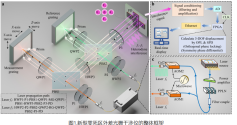
Li Xinghui's team proposed and verified an integrated zero-dead-zone heterodyne grating interferometer system, which uses a spatially symmetric dual-optical path architecture to eliminate the root cause of frequency and polarization aliasing errors, and built an error correction algorithm based on wavelet analysis and Butterworth filter to control the crosstalk error to less than 5%. The system adopts a compact design with an overall size of 90×90×40mm³, combined with a 3-DOF nano-piezoelectric platform, to achieve high-precision real-time multi-dimensional displacement measurement.
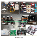
The experimental results show that the developed interferometer system can achieve a resolution of 0.25nm on the X/Y axis and 0.3nm on the Z axis, with a repeatability error better than 0.8nm and a linearity of up to 6.9×10⁻⁵. At the same time, it maintains a long-term stability better than 20nm (XY) and 60nm (Z) in a continuous test of 1000 seconds, and the measurement range reaches 10mm (XY) and 2mm (Z), respectively, with extremely high precision and wide range capabilities. This achievement has made an important contribution to the independent research and development of multi-dimensional high-precision measuring instruments in my country, and is expected to be widely used in strategic industrial fields such as high-end manufacturing equipment, advanced packaging, and quantum system control in the future.
Gallium Semiconductor (GARENSEMI) successfully prepared VB method 100mm (010) surface gallium oxide single crystal substrate
Gallium Semiconductor successfully grew a 100 mm gallium oxide single crystal using the vertical Bridgman (VB) method. After iterative process optimization, it successfully achieved the preparation of a 100 mm (010) surface gallium oxide single crystal substrate and carried out characterization tests. The test results showed that there were no twins in the substrate, the full width at half maximum (FWHM) of the XRD rocking curve of the single crystal substrate was less than 50 arcsec, and the surface roughness (RMS) of the substrate was less than 0.1 nm, and the quality reached the international advanced level .

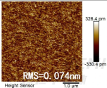
What are the advantages of choosing the (010) surface for gallium oxide growth?
Among the common mainstream crystal planes of gallium oxide single crystal substrates, the (010) substrate has excellent performance in physical properties and epitaxy:
1. (010) The substrate has the highest thermal conductivity, which is beneficial to improving the performance of power devices;
2. The (010) substrate has a faster epitaxial growth rate and good epitaxial matching, and is the preferred crystal plane for epitaxy.
At present, Gallium Ren Semiconductor has launched wafer-level (010) gallium oxide single crystal substrate products . This product is aimed at the scientific research market, meets the demand for (010) substrates in the scientific research field, and promotes collaborative cooperation between industry, academia and research.
Why use VB method to grow gallium oxide single crystals?
The VB method has significant advantages in the growth of gallium oxide single crystals and is becoming the new favorite in the industry. Domestic and foreign gallium oxide substrate manufacturers have begun to make plans.
Advantage 1 : The VB method is suitable for growing gallium oxide single crystals with the axis parallel to the [010] crystal direction, which is conducive to processing large-size (010) surface single crystal substrates.
Advantage 2 : The VB method does not use the precious metal iridium crucible, and there is no need to consider the oxidation loss of the crucible. Compared with the common growth method using iridium crucible, the cost is greatly reduced.
Advantage 3 : The VB method can use air atmosphere to grow single crystals, which can effectively inhibit the high-temperature decomposition of gallium oxide, reduce defects such as inclusions in the crystal due to crucible corrosion, and improve crystal quality.
Advantage 4 : The VB method has a small temperature gradient, and the number of dislocations induced by thermal stress in the crystal is small, so the crystal quality is high.
Advantage 5 : VB method crystals grow in a crucible, and the crystal diameter is the crucible diameter, so there is no need to control the crystal diameter. The technical difficulty is low and the stability is high, and it is easy to achieve automatic control.
What kind of equipment is used for growing gallium oxide by the VB method?
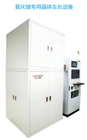
In September 2024, Gallium Ren Semiconductor launched the first self-developed gallium oxide dedicated crystal growth equipment, which not only meets the requirements of gallium oxide growth for high temperature and high oxygen environment, but also can perform fully automated crystal growth, reducing human intervention and significantly improving production efficiency and crystal quality. The equipment can obtain large-size single crystals with various crystal faces through process control, and supports the upgrade to larger-size single crystals, meeting the scientific research and production needs of universities, research institutes, and corporate customers for gallium oxide crystal growth. This type of gallium oxide VB method crystal growth equipment and its process package have been fully opened.
Kangda New Materials: Alumina targets have completed small batch verification! Domestic substitution has made further breakthroughs!
Regarding the alumina targets developed by the company, Kangda New Materials said: "Alumina targets can be used in the field of integrated circuit (IC) manufacturing to deposit insulating layers and dielectric layers, isolate circuits to prevent interference, reduce current leakage, and improve product reliability and durability.
At present, the alumina targets of the holding subsidiary Weixin Technology have completed small batch verification and are supplied according to customer order requirements." Target material - key material in semiconductor manufacturing process Sputtering targets are used in the sputtering thin film deposition process. Sputtering deposition is a physical vapor deposition (PVD) process, which uses energetic particles to bombard the material surface under a certain vacuum environment, so that particles are sputtered from the material surface and deposited on the substrate surface to form a thin film. The sputtering thin film deposition process has good repeatability and controllable film thickness. The prepared thin film has the advantages of high purity and good density. It can be used for the preparation of high-performance thin films in the integrated circuit industry, which plays an important role in promoting the development of the integrated circuit industry.
In the sputtering deposition process, the target material being bombarded is called the sputtering target. Sputtering targets can be used in many fields such as semiconductors, flat panel displays, photovoltaics, and record storage. In terms of classification: according to different shapes, sputtering targets can be divided into round targets, rectangular targets, and tubular targets. According to different materials, sputtering targets can be divided into pure metal targets (aluminum, titanium, copper, tantalum, etc.), alloy targets (nickel-chromium alloys, nickel-cobalt alloys, etc.), and ceramic compound targets (oxides, silicides, carbides, sulfides, etc.).
With an annual output of 1 million units! This SiC module production line is located in Guangdong Province
On June 10, according to the Zhongshan Torch Industrial Group, Basic Semiconductor (Zhongshan) Co., Ltd. (hereinafter referred to as "Zhongshan Basic") successfully won a 22-acre plot of land in the Shenzhen-Zhongshan Cooperation Zone, Minzhong Street, Torch High-tech Zone. This marks that Zhongshan's first silicon carbide module packaging production line construction project has officially settled in the Torch High-tech Zone.
On May 27, Basic Semiconductor officially submitted its listing application to the Hong Kong Stock Exchange, striving to become "China's first silicon carbide chip stock." On June 4, the Guangdong Provincial Investment Project Online Approval and Supervision Platform released the registration notice for the Zhongshan basic annual production of 1 million silicon carbide module packaging production line construction project. This major progress echoes the news of submitting a listing application to the Hong Kong Stock Exchange.
On June 10, Zhongshan successfully won the bid for the land for the packaging production line project. After completion, the annual production of silicon carbide power modules can reach 1 million, which will effectively promote the transformation and upgrading of the integrated circuit new materials and automotive parts industry in the Torch High-tech Zone. The "three strikes in a row" operation represents the determination of Basic Semiconductor to expand its core production capacity, and will provide strong support for the development of strategic emerging industries such as new energy vehicles, photovoltaic energy storage, etc. in the Guangdong-Hong Kong-Macao Greater Bay Area.
