Chinese semiconductor thread II

tokenanalyst

Brigadier
Registered Member

NAURA's patent for "process chamber for semiconductor equipment" published.​


Beijing North Huachuang Microelectronics Equipment Co., Ltd.'s "Process Chamber for Semiconductor Equipment" patent was published, the application publication date is February 14, 2025, and the application publication number is CN118422139A. =

527788895868.01514.jpg


The present application provides a process chamber of a semiconductor device, including a process chamber, a base, a protective lining and a grounding device; the base can be raised and lowered in the process chamber to support a wafer, the protective lining is arranged around the inner wall of the process chamber to protect the inner wall of the process chamber, and the grounding device includes a first connector, a second connector and a connecting spring, the first connector is connected to the base, the second connector is connected to the first connector through a connecting spring, and the second connector can fit with the protective lining to electrically connect the base and the protective lining. The first connector is electrically connected to the base, and when the base rises to the processing position, the connecting spring supports the second connector to fit with the protective lining, thereby realizing electrical connection between the base and the protective lining, so that the two are at the same potential, and arcing between the two is avoided. The connecting spring can be stretched and retracted multiple times without being damaged, thereby extending the service life of the grounding device.

Please, Log in or Register to view URLs content!
 

tokenanalyst

Brigadier
Registered Member

Harbin Institute of Technology proposes a new algorithm to accurately quantify the uniformity of CVD diamond nucleation!​


The distribution of particles is a topic that needs to be discussed in many research fields, and the field of CVD diamond is no exception. The uniformity of diamond nucleation is crucial to the quality and performance of CVD diamond, because the uniformity of CVD diamond in the nucleation stage directly affects the grain size, crystal orientation, stress and internal defect distribution of the diamond film.

At present, nucleation density is a quantitative index used by most researchers to describe the uniformity of diamond nucleation. This index is generally determined by counting the number of diamond nuclei per unit area of the substrate. However, nucleation density only gives an overall result. Imagine that if the diamond particles on the substrate only change in distribution but the overall number remains unchanged, the result given by the quantitative strategy based on nucleation density will not change. It can be said that people still lack effective quantitative evaluation methods for the uniformity of diamond nucleation.

Recently, the infrared thin film and crystal team of Harbin Institute of Technology proposed a new algorithm that uses Kullback-Leibler (KL) divergence to quantitatively evaluate the uniformity of CVD diamond nucleation, effectively overcoming the limitations of traditional indicators (such as nucleation density, which focuses too much on the whole and the variance is easily affected by outliers). The new algorithm was evaluated by comparing five groups of silicon substrates with different diamond nucleus distributions and changing the partition size.

Please, Log in or Register to view URLs content!
 

tokenanalyst

Brigadier
Registered Member
New EUV photoresist chemical supplier company​

Light Chaser--Domestic Supplier of Fluorinated Photoinitiators for EUV Photoresists​

EUV extreme ultraviolet photoinitiator is a strategic material and one of the important supporting additives for photoresist . It can be used to prepare high-specification chips below 3nm . It is not only the cornerstone of new industrial development, but also the guarantee for the manufacturing of important national defense equipment . However, the global semiconductor EUV photoinitiator market is mainly monopolized by foreign manufacturers such as Japan (JSR) and Tokyo Ohka . As the world's largest chip consumer market, China's current domestic self-sufficiency rate for EUV photoinitiators is almost 0. At present , no company in China can independently develop the initiator . In 2024 , China 's EUV photoinitiator market will reach US$ 67 billion, and it will grow at a rate of 67.9%.

The project leader, has 5 years of experience in R&D in the photoresist raw materials industry and many years of experience in family management . During the process, he found that the current EUV photoresist initiators on the market have three major technical pain points, such as poor photosensitivity, short storage period, and difficulty in removing residual glue after adding to the photoresist.

Relying on platforms such as the Changzhou University National Experimental Center for Chemical Engineering and the "Joint Laboratory for High-Resolution Lithography Basic Materials Technology" jointly built with Nanjing University Optoelectronics, the team has developed the first EUV photoinitiator with independent intellectual property rights in China. The photosensitivity reaches the highest level 5 in the industry, the storage period is doubled compared to Japan's JSR (6 months), and the advantages of low residual glue have broken the years of monopoly of Japan's JSR and Tokyo Ohka , filling the gap in the domestic market . The team has deployed 25 invention patents to protect the technology, and 15 papers related to the project technology have been included in the American Chemical Society (ACS) and the Royal Society of Chemistry (RSC), one of which was published as a cover article in Advanced Science ( the influence of the photolithography materials industry is second only to Science and Nature). At present, the EUV photoinitiator developed by the team is backward compatible with DUV, G-line and I-line lithography equipment, and can bypass the EUV lithography machine of AMSL in the Netherlands. Second-tier customers can produce high-specification chips using domestic equipment and photoresists .

The team is based in Suzhou Industrial Park , a national-level "integrated circuit industry metropolitan area", and established Jiangsu Zigancai New Materials at the end of May 2025. At present , the product has received formal orders from domestic photoresist leaders Jiangsu Nanda Optoelectronic Materials Co., Ltd. (Stock Code: 300 346 ) and Changzhou Qiangli Electronic New Materials Co., Ltd. (Stock Code: 300429 ). In addition, the team has obtained shares from industrial capital (Changzhou Edsent Polymer Technology Co., Ltd.) and social capital with Suzhou government fund background (Suzhou Xinheng Yinqi Investment Co., Ltd.) .​
 

tokenanalyst

Brigadier
Registered Member

Simulation study on the state parameter distribution and extreme ultraviolet radiation of laser tin plasma​


The laser tin (Sn) plasma light source is the core subsystem of the current advanced extreme ultraviolet (EUV) lithography machine. The power value and stability of the EUV light within the 2% bandwidth around 13.5 nm are one of the key indicators to determine the success of the entire lithography machine. This paper conducts a detailed numerical simulation study on the distribution of plasma state parameters and EUV radiation spectrum for the complex system of laser Sn plasma light source. Firstly, based on the detailed energy level model, the Sn plasma is calculated under the condition of local thermodynamic equilibrium approximation in the range of 12-16 The radiation opacity data of the nm band was obtained. Then, the laser plasma radiation fluid dynamics program RHDLPP was used to simulate the distribution of state parameters such as temperature and electron density of the plasma generated by the nanosecond laser pulse acting on the Sn plane solid target and the droplet target. Combining the radiation opacity data and plasma state data, the spectral simulation post-processing subroutine SpeIma3D was used to complete the simulation of the spatially resolved EUV spectrum of the plane target plasma and the angularly resolved EUV spectrum of the droplet target plasma at an observation angle of 60°. Finally, the variation law of the intra-band radiation intensity of the droplet target plasma within the bandwidth of 13.5nm and 2% with the observation angle was obtained. All plasma state parameter distributions and EUV spectrum simulation results obtained in this paper are in good agreement with the existing experimental results, which proves the simulation ability of the RHDLPP program in laser Sn plasma EUV light source. The relevant results can provide certain support for EUV lithography and the development of domestic EUV light sources.

Please, Log in or Register to view URLs content!
 

tokenanalyst

Brigadier
Registered Member
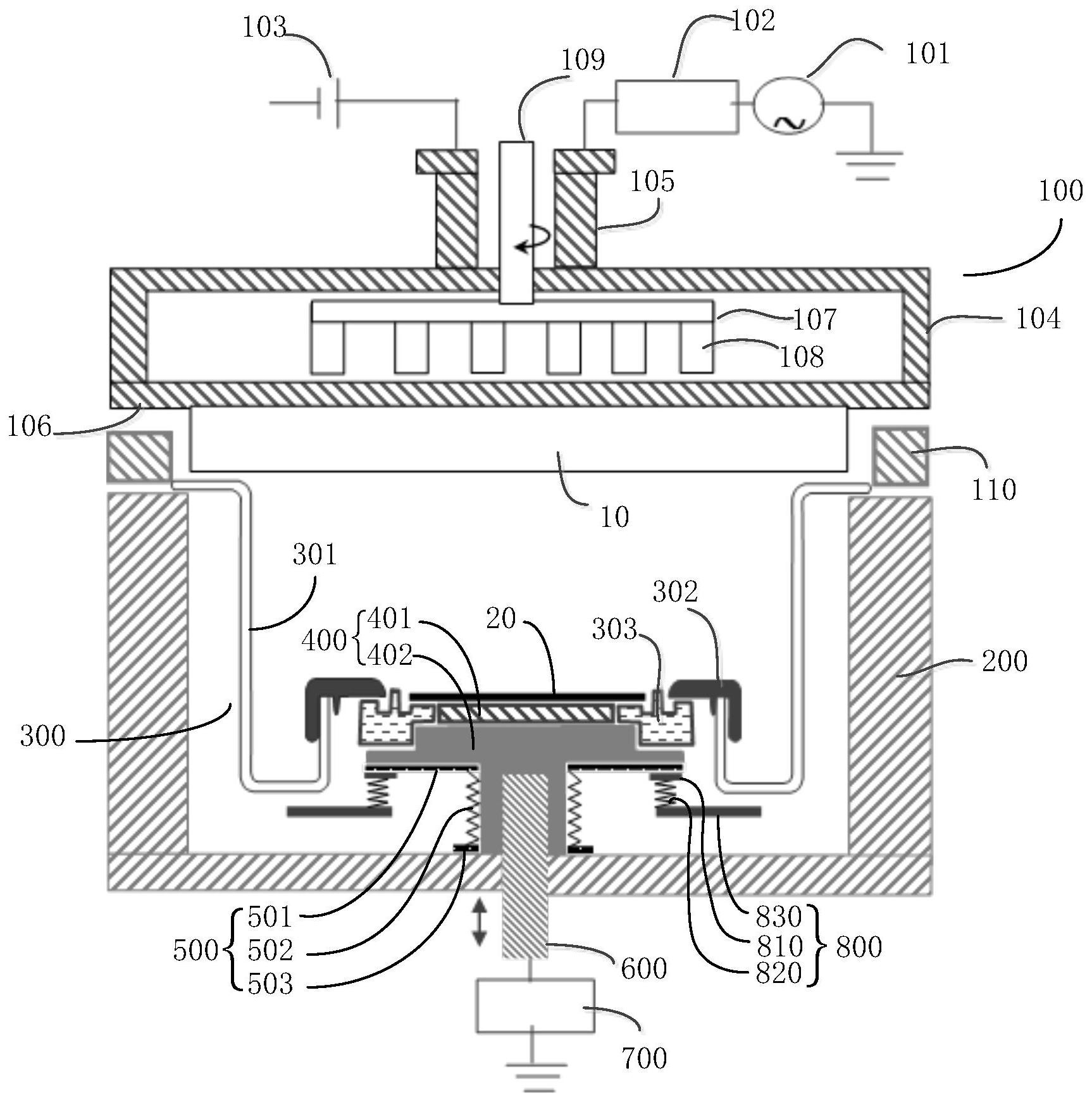
Temperature control for lithography machines.

Airsys temperature control innovation overcomes overseas technical barriers and leads the rise of domestic products.​


In 2025, the localization rate of China's semiconductor equipment is expected to reach 35%-50%. In response to national policies, AIRSYS promotes the localization transformation of the semiconductor industry and injects new impetus into China's semiconductor industry with its innovative breakthroughs in wafer-level precision temperature control modules.

1749746857649.png

The core advantages of AIRSYS temperature control technology

1. High-precision temperature control module

The precision temperature control module developed by AIRSYS is suitable for wafer processing and is designed for the core process of semiconductor manufacturing, covering key steps such as photoresist coating and wafer inspection. The module uses advanced sensor technology and intelligent control system to achieve high-precision temperature control of ±0.005℃, ensuring process stability and repeatability. Its unique dual-channel design enables the equipment to quickly switch temperature ranges at different process stages to meet diverse needs from low temperature to high temperature.

2. Technological breakthrough: full-chain innovation from algorithms to materials

AIRSYS has always maintained a large investment in innovation and research and development, and has continuously introduced efficient cooling/heating technologies and advanced algorithms, allowing temperature control equipment to reach international leading levels in terms of accuracy, stability and energy efficiency. At the same time, AIRSYS also provides customized solutions to tailor the most suitable temperature control system according to the process requirements of different customers. This "technology + service" dual-wheel drive model is reshaping the competitive landscape of China's temperature control equipment market.

3. Reliability and stability

In semiconductor manufacturing, reliable equipment and stability are essential. Airsys' temperature control equipment uses special low-temperature alloy materials and modular antifreeze design. The core parts can withstand extreme environments, ensuring the reliability and durability of the equipment under high-load operation. The equipment is also equipped with different safety protection mechanisms, which can monitor the operating status in real time, quickly warn and handle faults, and ensure the continuity of the production process.

4. Market recognition of AIRSYS temperature control technology

AIRSYS's temperature control technology is highly reliable and innovative, and has been widely recognized by domestic semiconductor production lines. Not only has the product achieved significant sales in the domestic market, it has also attracted the attention of many internationally renowned companies. At the SEMICON China 2025 exhibition, AIRSYS attracted a large number of industry elites to stop and negotiate with its ±0.005℃ ultra-precision temperature control technology and AI-driven digital management platform, and won a lot of cooperation intentions. Many of the world's top 10 semiconductor companies made a special trip to visit the AIRSYS exhibition area to communicate and exchange technical advantages and service systems, which consolidated AIRSYS's core position in the industrial chain.

-------------------------

Interesting:

According to "Made in China 2025", clear requirements are put forward for the localization of semiconductor equipment:

As of 2020

Achieve a 50% localization rate for 90-32 nanometer process equipment, a 50% localization rate for key packaging and testing equipment, and a 90 nanometer lithography machine

By 2025

Achieve 30% localization rate of 20-14 nanometer process equipment and localization of immersion lithography equipment

By 2030

Realize the localization of process equipment, EUV lithography equipment, and packaging and testing equipment

In 2025, the localization rate of China's semiconductor equipment is expected to reach 35%-50%. In response to national policies, AIRSYS promotes the localization transformation of the semiconductor industry and injects new impetus into China's semiconductor industry with its innovative breakthroughs in wafer-level precision temperature control modules.
 

Michael90

Junior Member
Registered Member
Nexchip already surpassed its Taiwanese parent company PSMC in revenue.
I expect not only SMIC to surpass Samsung foundry, but for Hua Hong to surpass GlobalFoundries this decade.
Nexchip is a Taiwanese company?
Chinese foundries are doing well, I guess their growth will speed up this decade as the country's te h companies have no choice but to rely on them for their chips due to sanctions, which is a good thing for these companies.
Crazy to see how dominant TSMC from Taiwan is. They are twice as much as all the following top 9 combined. That's crazy. It's almost like a monopoly. It's a good thing more competitors are emerging from China. I thought Samsung could match TSMC but seems that's a distant dream.
 

sunnymaxi

Major
Registered Member
Gree announced that its SiC factory has achieved mass production!

Its 6-inch SiC chip factory located in Zhuhai High-tech Zone, as Asia's first fully automated IDM (vertically integrated manufacturing) factory, took only 388 days from the groundbreaking ceremony in July 2022 to the opening of the line in December 2024, setting a new record for the construction speed of domestic semiconductor factories. The total investment of the factory is 5.5 billion yuan, covering an area of 200,000 square meters, with an annual production capacity of 240,000 SiC wafers. The current yield rate is stable at 99.6%, and the single-chip manufacturing cost is 18% lower than the industry average.

In addition, Gree plans to promote the application of SiC chips in core areas such as photovoltaic inverters and electric vehicles in 2025. By building its own SiC chip factory, Gree has successfully integrated SiC materials, devices, applications and other links, forming a strong internal synergy effect, effectively reducing costs and improving supply chain stability..

Please, Log in or Register to view URLs content!
 

huemens

Junior Member
Registered Member

US says China's Huawei can't make more than 200,000 AI chips in 2025​

Please, Log in or Register to view URLs content!

"Our assessment is that Huawei Ascend chip production capacity for 2025 will be at or below 200,000 and we project that most or all of that will be delivered to companies within China," Jeffrey Kessler, Under Secretary of Commerce for Industry and Security at the Commerce Department, told a congressional hearing.
"China is investing huge amounts to increase its AI chip production, as well as the capabilities of the chips that it produces. So, it's critical for us not to have a false sense of security, to understand that China is catching up quickly," he told the House of Representatives Foreign Affairs South and Central Asia subcommittee.
Kessler said he was not planning any immediate new restrictions on U.S. semiconductors sold to China, but that the Commerce Department will "remain active in this space."
 
Top