The Biden administration laid out an ambitious new goal for the US: produce 20% of the world’s most advanced semiconductor chips by 2030. Achieving that mark — set by Commerce Secretary Gina Raimondo in a speech Monday morning — would be a dramatic turnabout for the US. It currently makes 0% of the so-called "leading edge logic" chips.
You are using an out of date browser. It may not display this or other websites correctly.
You should upgrade or use an alternative browser.
You should upgrade or use an alternative browser.
Chinese semiconductor thread II
- Thread starter vincent
- Start date
240,000 pieces! Another 6-inch SiC epitaxial wafer project started
Information on the official website of Hebei Puxing Electronic Technology Co., Ltd. (hereinafter referred to as Puxing Electronics) showed that the company’s “6-inch low-density defective silicon carbide epitaxial wafer industrialization project” conducted its first environmental impact assessment information disclosure ( (hereinafter referred to as the announcement).
The announcement shows that the total investment in this project is 350.7016 million yuan. The company's No. 1 factory building will be used for reconstruction and expansion, with a construction area of about 4,000 square meters. 116 silicon carbide (SiC) epitaxial equipment and supporting equipment will be purchased to form a 6-inch low-density defective SiC Epitaxial material production line. After the project is completed, it will achieve an annual production capacity of 240,000 SiC epitaxial wafers .According to the official website of Puxing Electronics, the company was founded in November 2000 and is committed to the epitaxial research, development and production of high-performance semiconductor materials. It is a holding subsidiary of China Electronics Semiconductor Materials Co., Ltd. (hereinafter referred to as Dianke Materials). Puxing Electronics' main products are silicon-based epitaxial wafers, gallium nitride (GaN) and SiC epitaxial wafers of various specifications and models, which can be widely used in clean energy, new energy vehicles, aerospace, automobiles, computers, tablets, smart phones, etc. Mobile phones, home appliances and other fields.In recent years, Puxing Electronics, a subsidiary of Dianke Materials, has actively deployed the R&D and production of third-generation semiconductor epitaxial materials. In September 2021, it launched a new epitaxial material industry base construction project covering an area of 130 acres and completed it in April 2022. The main factory building was capped, and the first batch of production and inspection equipment was moved in in September. In November, the first silicon epitaxy and SiC epitaxy rolled off the production line, marking that the industrial base officially entered the trial production and verification stage.It is reported that in April 2022, Puxing Electronics also announced a "6-inch silicon carbide epitaxial wafer industrialization project". The total investment of this project is 180 million yuan. It rents the existing equipment of Tonghui Company (affiliated to the 13th Institute of China Electronics Technology) Plant, purchased 15 SiC epitaxial furnaces and supporting testing instruments, etc., completed the construction of a 6-inch SiC epitaxial wafer mass production line, and achieved an annual production capacity of 60,000 6-inch SiC epitaxial wafers.
more related to the DPP than mainland China.
The Biden administration laid out an ambitious new goal for the US: produce 20% of the world’s most advanced semiconductor chips by 2030. Achieving that mark — set by Commerce Secretary Gina Raimondo in a speech Monday morning — would be a dramatic turnabout for the US. It currently makes 0% of the so-called "leading edge logic" chips.
If they succeed, which I don't think they will, but if they succeed is going to be at the expense of the Taiwanese semiconductor industry, if the Japanese succeed, which is more likely, is going to be at the expense of the Taiwanese semiconductor industry, If the Germans succeed, who may or may not, is going to be at the expense of the Taiwanese semiconductor industry. So basically the DPP is only good for being trouble makers lapdogs and prostituting that island most successful product: Semiconductors.
Microwave Photonics Team of the Xi'an Branch of the Fifth Aerospace Academy: Breakthrough in high-performance on-chip integrated photonic Repeater technology
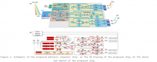
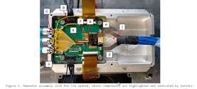
In response to the technological development needs of spaceborne flexible processing and reconfigurable switching and forwarding, the team of researcher Tan Qinggui from the Xi'an Branch of the Fifth Academy of Aerospace Science and Technology Group proposed a spaceborne microwave photon Repeater chip technology solution based on InP and Si 3 N 4 hybrid integration to achieve multi-channel Photonic frequency conversion and narrowband channelization functions. For the first time, this technical solution achieves full-chip integration of dual-gain external cavity lasers, array MZM modulators, array SOA amplifiers, broadband optical filters, and narrowband optical channelizers. Based on this technical solution, the research team designed and completed the development of the spaceborne microwave photon Repeater chip, which achieved 2GHz bandwidth Ka-K band down conversion and 4-channel 500MHz granularity Flat-top narrowband optical channelization filtering, verifying the microwave photon technology’s wideband flexible RF signal processing capabilities.
The research results were published in the 2024 issue 2 of the international optical journal Laser& Photonics Reviews under the title "Chip-Based Microwave Photonic Payload Repeater for High Throughput Satellites". Dr. Liang Dong from the Xi'an Branch of the Fifth Aerospace Academy is the first author of the paper, and Researcher Li Li and Researcher Tan Qinggui are the corresponding authors of the paper.

The radio frequency channel processing target of current high-throughput satellite payloads is high-frequency continuous signals with an instantaneous bandwidth not exceeding 5GHz. In order to connect with subsequent digital signal processing components and high-power amplifier components, the broadband signal needs to be divided into multiple narrowband signals with continuous bandwidths of hundreds of MHz. The signal multiplexing and processing of traditional optical communications and microwave photonics technology are mostly performed at the sub-nm scale. For example, the commonly used 1550nm band DWDM spacing is 0.8nm (100GHz), and the smallest single WDM filter bandwidth is 0.4nm (50GHz). There is a huge gap between spaceborne radio frequency processing requirements and traditional photonic signal processing capabilities. At present, traditional satellite applications still rely on frequency-sensitive microwave passive multiplexers to achieve on-board channel division functions. For microwave photonic systems with typical carrier frequencies around 193THz, building a FLat-Top narrowband optical filter with a filter bandwidth close to 1GHz is still a big challenge.

The hydrogen and helium separation device can extract high-purity helium with a purity of more than 99.999%
The reporter learned on the 21st that the hydrogen and helium separation and purification device independently developed by China Youyan Group Youyan Engineering Technology Research Institute Co., Ltd. (hereinafter referred to as Youyan Industrial Research Institute) has recently been successfully applied to helium extraction from natural gas flash gas (BOG) in Luliang, Shanxi. The first phase of the project has successfully produced high-purity helium with a purity of over 99.999% after undergoing long-term and low-temperature operation tests. This marks important technological progress in the field of domestic helium extraction.

Relevant statistics show that my country’s helium resources account for only 2% of the world’s total. As a major helium consumer, my country ranks second in the world in demand for helium, especially in aerospace, electronics, biomedical and other fields.
"Currently, the only industrial production method of helium is extraction from natural gas. To solve the problem of separation of helium and hydrogen, two small molecule gases in the helium refining process, Youyan Industrial Research Institute innovatively uses adsorption dehydrogenation. The safe and efficient separation of the two gases has been achieved." Hao Lei, deputy general manager of Youyan Industrial Research Institute and general manager of the New Energy Division, said that this method has significant advantages over other technologies in terms of gas purity and safety.
Hao Lei introduced that the newly developed hydrogen and helium separation device can be easily integrated into various BOG helium extraction systems, and can achieve coarse separation, refinement and purification of helium in a normal temperature environment. The purity of the helium output gas can reach more than 99.999%. , and at the same time, hydrogen products with a purity higher than 99.999% can be obtained. This technology maximizes the application of natural gas resources and provides a new way to obtain helium resources. It is of great significance for improving the utilization rate of my country's helium resources, reducing helium external dependence, and ensuring the safety of my country's helium use.
It is reported that over the years, Youyan Industrial Research Institute has been deeply involved in the field of gas purification. It has developed the first hydrogen purification system for hydrogen-cooled generators in China, realizing its application and promotion in domestic thermal power stations; it has developed various specifications of alloy purifiers, palladium membranes Products such as purification devices and gas separation devices are used in fields such as electric power and semiconductors.
Moore Threads MTT S4000 48GB AI GPU: with MTLink and zero-cost NVIDIA CUDA framework.
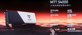
Moore Threads has just announced its new MTT S4000 AI GPU that will work "seamlessly" with NVIDIA's CUDA framework, thanks to an in-house MUSIFY translation tool.
The new Moore Threads MTT S4000 AI GPU features MTLink 1.0, which is a new multi-GPU connector that we don't have photos of, but it sounds similar to NVIDIA's in-house NVLink connector. The new MTT S4000 AI GPU has 48GB of GDDR6 memory with up to 768GB/sec of memory bandwidth, compared to the 48GB of memory on NVIDIA's RTX 6000 GPU with 960GB/sec of memory bandwidth.

Moore Threads is passively cooling its new MTT S4000 AI GPU, with 25 TFLOPs of FP32 single-precision compute performance, 100 TFLOPs of FP16/BF16, and 200 TOPS in INT8. This is all found on a PCIe Gen5 x16 connector, too.
Moore Threads has made its new MTT S4000 AI GPU with larger customers in mind, who are wanting to have a KUAE Smart COmputing Center Solution. It's a full GPU-based stack for large-scale computing that the Chinese company can deploy in only 30 days. The GPU server supports 70 billion to 130 billion parameters training for Large Language Models (LMMs).
Moore Threads explained on its website: "In the era of large models, intelligent computing power represented by GPU is the cornerstone and the center of the generative AI world. Moore Thread cooperates with China Mobile Beijing Company, China Telecom Beijing Branch, Lenovo, 21Vianet, Halo New Network, Zoomlion Data, Shudao Intelligent Computing, China Development Intelligence Source, Qishang Online, Nortel Digital Beijing Digital Economy Computing Power More than ten companies including the Center, Ziguang Hengyue, Ruihua Industrial Holdings (Shandong), Saier Network, Zhongke Financial, Zhongyun Intelligent Computing, Jinzhou Yuanhang (in no particular order), jointly announced the "Moore Thread PES - KUAE Intelligent Computing Alliance" was established".
"The alliance will vigorously build and promote a national industrial intelligent computing platform from underlying hardware to software, tools and applications, aiming to achieve high utilization of clusters and become the first choice for large model training with easy-to-use, full-stack intelligent computing solutions".
Another stupid article, maybe a problem for some other fabs and design houses but SMIC and HHGrace have their own photomask shops for quite some time.Taiwan threaten to ban photomask exports to China for chip up to 14nm.
Sirui Intelligent signed an ALD equipment purchase agreement with Innosec
Qingdao Sifang Sirui Intelligent Technology Co., Ltd. (hereinafter referred to as "Sirui Intelligence") signed a new ALD equipment purchase agreement with the world's leading GaN IDM manufacturer Innosec Technology Co., Ltd. (hereinafter referred to as "Innosec") protocol. According to the agreement, Sirui Intelligent will supply Innosec with Transform series mass-production ALD deposition coating equipment for the front-end process of gallium nitride semiconductor wafer manufacturing, supporting its 8-inch silicon-based gallium nitride wafer production line. expansion.
Third-generation semiconductor power devices such as GaN and SiC are the key to achieving higher power conversion efficiency. Research institute Yole Développement predicts that the market size of GaN power devices is expected to reach US$2 billion by 2027. At the same time, the growing demand for gallium nitride semiconductor products in consumer electronics, data centers, mobile travel, industrial Internet, new energy and other fields has promoted the performance upgrade of emerging semiconductor material gallium nitride and entered rapid development. period.
作为一种通用型技术,ALD镀膜工艺对于氮化镓功率器件的性能提升有着显著的增益。例如ALD薄膜可用于高质量的栅极介电叠层,有助于提升器件击穿电压、漏电抑制和阻水疏氧效果。Transform系列量产型ALD沉积镀膜设备,是思锐智能拥有近40年ALD技术积累的集大成者,支持配置多个ALD工艺模块,兼容热法及等离子体功能,可为应对不断增长的产能和新的应用而进行升级,目前已进入欧洲、北美、日本和中国大陆及台湾地区知名厂商,并实现重复订单。Innosec is the world's leading GaN IDM manufacturer, dedicated to the R&D and manufacturing of third-generation semiconductor gallium nitride on silicon (GaN-on-Si). It has the world's largest 8-inch gallium nitride on silicon wafer production capacity. Product design and performance are at the internationally advanced level. The cumulative shipments of its high- and low-voltage full-power gallium nitride chips have exceeded 250 million units and are widely used in cutting-edge fields such as consumer electronics, server power supplies, automotive electronics, and new energy.Sirui Intelligent is very much looking forward to joining hands with Innosec to jointly promote the gallium nitride industry, China's "dual carbon" goal and sustainable development. Sirui Intelligent is also accelerating product development and market verification in more fields, actively deploying other front-end equipment businesses, providing more value to customers, and striving to become the backbone of the development of the global semiconductor industry.
