Chinese semiconductor thread II

tokenanalyst

Brigadier
Registered Member

Investing 628 million yuan! Vogel's 8.6-generation OLED photolithography project settled in Chengdu.​


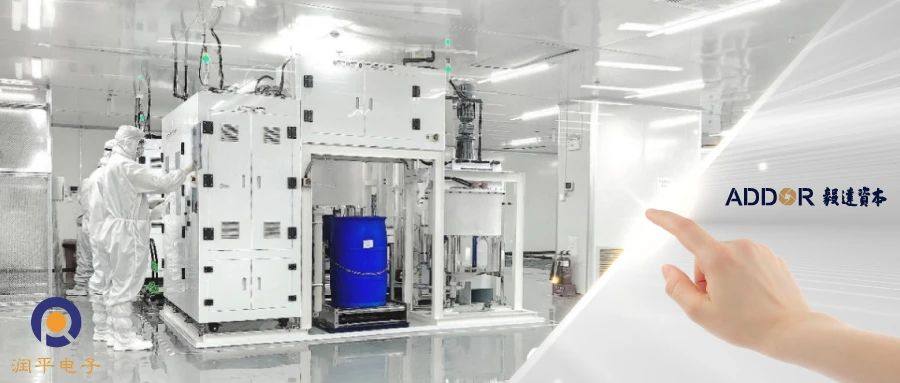
According to reports, the total investment of Chengdu Vog Optoelectronics AMOLED photoetching project is 628 million yuan, and it is planned to build an automated production plant of 77,000 square meters, mainly serving the glass substrate back-end process of AMOLED display screens. After the project is put into production, it will use the ECI technology independently developed by Vog Optoelectronics to achieve integrated breakthroughs in processes such as thinning of medium and large-sized AMOLED glass substrates and selective pattern etching, and provide high-precision supporting services for the first 8.6-generation OLED production line in China.

The launch of this project marks a further step forward in Vog Optoelectronics' strategic layout in the field of new display. In the future, the company plans to rely on the industrial agglomeration advantages of Chengdu Hi-tech Zone to continue to expand application scenarios such as smart terminals and in-vehicle displays, and help Chengdu Hi-tech Zone's new display industry move towards high-end and internationalization.

"The implementation of the Chengdu Voger AMOLED photo-etching project is an important measure for Chengdu Hi-tech Zone to deepen the layout of the new display industry chain and create the 'World Soft Valley'." A relevant person in charge of the Electronic Information Industry Bureau of Chengdu Hi-tech Zone said that the global display industry is currently accelerating the iteration of AMOLED technology. Chengdu Hi-tech Zone will rely on leading companies such as BOE to continuously improve the "materials-equipment-panel-terminal" full-chain ecology, help companies break through the bottleneck of localization of key supporting technologies, and provide solid support for Chengdu to build a national new display industry cluster.

In recent years, Chengdu Hi-tech Zone has focused on the two major sub-sectors of flexible display and Micro-LED. Around chain-leading enterprises such as BOE, it has gathered more than 40 upstream and downstream enterprises above the designated size, covering core supporting links such as glass substrates, photomasks, and testing equipment, forming a complete industrial ecology with chain-related enterprises such as China Optoelectronics, Messer, Luwei Optoelectronics, and Huaxing Yuanchuang taking root in the local area.

Please, Log in or Register to view URLs content!
 

tokenanalyst

Brigadier
Registered Member

Performance improved by 40%! Researchers achieve major breakthrough in DUV\xa0LED field​


Researchers from Wuhan University in China introduced a breakthrough in the field of DUV LED in the journal Nano Letters, titled " Aluminum Gallium Nitride ( AlGaN ) Polarized Ultrathin Tunnel Junction Deep Ultraviolet Light-Emitting Diode " . According to reports, they solved a long-standing problem in the field of deep ultraviolet (DUV) light-emitting diode (LED) research through the development of a technology called polarized ultrathin tunnel junction (PUTJ) . Sample test results showed that they achieved a record low operating voltage of 5.8 volts at a driving current density of 30 amperes per square centimeter , while at the same time, the light output power ( LOP , Light Output Power ) of the deep ultraviolet light-emitting device increased by 40%.

1744213468630.png

The research team said that the achievement was mainly due to their use of a polarized aluminum gallium nitride heterostructure , which can greatly improve the tunneling of carriers and current diffusion in the device . This also marks an important step forward in the development of efficient deep ultraviolet light sources for sterilization, sensing and medical use by the academic community .

Shengjun Zhou, who led the research , said: "By reducing the thickness of the device's tunnel junction and strategically controlling the aluminum content in the middle layer, we have successfully achieved dual optimization of the two indicators of vertical tunneling efficiency and current spreading. Here, the polarization electric field we added at the heterojunction eventually narrowed the depletion region, and the tunneling probability of this new design was increased by 1.5 times compared to the traditional ultrathin tunnel junction (UTJ) . At the same time, the higher resistance of the middle layer also helps to improve the internal current diffusion when large-size light-emitting devices are working . "

In fact, deep ultraviolet LEDs are facing some important bottlenecks in current commercial applications , including : light loss due to p -type gallium nitride (p-GaN) absorption, and high operating voltage due to poor hole injection in high aluminum content aluminum gallium nitride. To solve this problem, previous researchers proposed a traditional tunnel junction design, which can alleviate the above absorption problem, but because of the thicker n-type aluminum gallium nitride current diffusion layer, it increases the body resistance of the entire device.​

Please, Log in or Register to view URLs content!
 

tokenanalyst

Brigadier
Registered Member

GigaDevice expects Q1 revenue to be 1.909 billion yuan, a year-on-year increase of 17.32%​

GigaDevice announced that according to preliminary estimates by the company's financial department, the company expects operating income to be around 1.706 billion yuan in the fourth quarter of 2024 and 1.909 billion yuan in the first quarter of 2025. The operating income in the first quarter of 2025 will increase by about 282 million yuan compared with the same period last year, a year-on-year increase of about 17.32%, and a month-on-month increase of 203 million yuan compared with the fourth quarter of 2024, achieving a month-on-month increase of about 11.88%.

Regarding the reasons for the performance growth, GigaDevice pointed out that the demand in the downstream market of the semiconductor industry in which the company is located has recently rebounded. In the first quarter of 2025, benefiting from the national stimulus package and other reasons, the demand in the consumer field was boosted; benefiting from the demand for storage capacity driven by terminals such as AIPC, the company's products achieved a significant increase in revenue and sales in the storage and computing fields; the network communication market also achieved good growth.

In terms of operations, GigaDevice continues to maintain a market share-centered strategy, continuously increases R&D investment and product iteration, continuously optimizes product costs, enriches the product matrix, and continuously enhances the competitiveness of the company's multiple product lines.

Please, Log in or Register to view URLs content!
 

tokenanalyst

Brigadier
Registered Member

Runping Electronics has completed an investment of tens of millions of yuan to help domestic wafer "nano-level flatness" break through again​


Recently, Yida Capital completed an investment of tens of millions of yuan in Shanghai Runping Electronic Materials Co., Ltd. (hereinafter referred to as "Runping Electronics") . This round of financing will be used for the company's product research and development, team expansion, etc., to continue to expand the company's influence.

Runping Electronics was established in 2021 and focuses on the research, development, production and sales of CMP polishing materials for semiconductor chip manufacturing. Its main products include polishing pads, slurries, retainer rings, membranes, ultra-high precision polishing heads, etc. The company's products have been supplied in batches to domestic 12-inch head memory chip factories and logic chip factories, making it one of the industry's leading core suppliers of CMP polishing materials.


10d9c0e8bd873a42b0d724d00b9fcb89.jpeg!a

The CMP process, also known as chemical mechanical planarization technology, is widely used in three major fields: silicon wafer manufacturing, wafer manufacturing, and advanced packaging. It is a key process for achieving wafer surface flatness and chip miniaturization in the integrated circuit manufacturing process. With the continuous advancement of process nodes, the number and density of multi-layer wiring increase, the number of wafer polishing steps continues to increase, and the demand for polishing materials grows rapidly. The number of polishing times for 7nm process chips can reach more than 30 times.

Runping Electronics was incubated by Jiangfeng Electronics (300666.SZ), and the core members of the team have worked for global CMP material leaders such as Cabot. As a national science and technology-based small and medium-sized enterprise focusing on CMP polishing materials, relying on the industrial platform support of Jiangfeng Electronics, Runping Electronics has obtained more than 32 patent authorizations. The management team has created a leading domestic CMP polishing material solution with more than ten years of experience in the field of semiconductor materials.

The company has achieved batch shipments in the field of polishing pads and has established a domestic polishing pad production line; in the polishing liquid category, it has multiple product lines such as polysilicon polishing liquid, oxide polishing liquid, metal tungsten polishing liquid and cerium oxide polishing liquid. Among them, polysilicon polishing liquid has achieved 100% localization of the entire chain from polishing particles to final products. In the field of polishing head maintenance services, the company has become one of the largest core component suppliers in China. Runping Electronics aims to serve customers in the semiconductor chip manufacturing field well. By building a diversified product matrix, it realizes the localization of the entire chain of CMP polishing materials, demonstrating its foresight and responsibility in strengthening supply chain security.

Please, Log in or Register to view URLs content!
 

tokenanalyst

Brigadier
Registered Member

New progress in Silan Micro's SiC project, 6/8-inch dual-line operations​

On April 8, Silan Microelectronics released an announcement disclosing the latest progress of Silan Microelectronics' silicon carbide (SiC) project. Remarkable results have been achieved in both the research and development of SiC chip technology and mass production, with capacity construction and technological breakthroughs going hand in hand.

"Silan Minggai 6-inch SiC power device chip production line" project: capacity release

As of now, Silan Microelectronics has formed a monthly production capacity of 9,000 6-inch SiC MOS chips. The electric vehicle main motor drive module produced based on Silan Microelectronics' self-developed second-generation SiC-MOSFET chips has cumulatively shipped 50,000 units to four domestic automobile manufacturers. With the release of the production capacity of the 6-inch SiC chip production line, mass production and delivery have been achieved.
At present, Silan Microelectronics has completed the development of the Ⅳ generation planar gate SiC-MOSFET technology, and its performance indicators are close to the level of trench gate SiC devices. The Ⅳ generation SiC chips and modules have been sent to customers for evaluation, and power modules based on the Ⅳ generation SiC chips are expected to be mass-produced in 2025.​

"Silan Jihong 8-inch SiC power device chip production line" project: line is completed

As of now, Silan Jihong's 8-inch SiC mini line has been put into production, and Silan Microelectronics' second-generation SiC chip has been successfully taped out on the 8-inch mini line. Its parameters match Silan Microelectronics' 6-inch products, and the yield rate is significantly higher than that of 6 inches.
The main factory building and other buildings of Silan Jihong have been fully topped off and are undergoing purification and decoration. It is expected to be fully operational and start trial production in the fourth quarter of 2025 to catch up with the rapid growth of the automotive SiC market in 2026.

Public information shows that after the Silan Jihong project reaches full production, it will be able to meet more than 40% of the domestic demand for automotive-grade SiC chips, and drive the upstream and downstream industrial chains to gather in Xiamen, accelerating the localization process of third-generation semiconductor materials and equipment.

Please, Log in or Register to view URLs content!
 

interestedseal

Junior Member
Registered Member
Most of US brand semiconductors and equipments aren't even made in the US,so I don't expect much impact on this
Please, Log in or Register to view URLs content!

Latest clarification on country of origin definition for semi
Pretty important since semis are the largest source of trade deficit for China
Country of origin=country of fabbing/taping out
So Intel/Micron/analog companies most affected
 

OptimusLion

Junior Member
Registered Member
High numerical aperture illumination lithography mask for super-resolution lithography and preparation method thereof, lithography method

Screenshot_2025-04-11-11-57-47-34_40deb401b9ffe8e1df2f1cc5ba480b12.jpg

Deep ultraviolet super-resolution interference lithography method based on surface plasmons

Screenshot_2025-04-11-11-58-48-08_40deb401b9ffe8e1df2f1cc5ba480b12.jpg

Area-selective deposition method for optimizing pattern quality in super-resolution lithography

Screenshot_2025-04-11-12-04-43-75_40deb401b9ffe8e1df2f1cc5ba480b12.jpg
 
Top