Chinese semiconductor thread II

tokenanalyst

Brigadier
Registered Member

Fuga Gallium Industry has made a breakthrough in gallium oxide MOCVD homoepitaxial technology, helping the downstream vertical power electronic device industry to land​


Recently, Hangzhou Fuga Gallium Technology Co., Ltd. (hereinafter referred to as Fuga Gallium), an incubated enterprise of the Hangzhou Institute of Optics and Fine Mechanics, has made important technological breakthroughs in the research and development of gallium oxide MOCVD homoepitaxial thin films. It has homoepitaxially grown a thin film with a thickness of more than 10 microns on Fuga Gallium's gallium oxide single crystal substrate. Verified by national authoritative testing agencies, this technology has reached the international leading level. Related standardized products will be launched in April 2025, providing key material support for high-end equipment such as new energy vehicle high-voltage platforms and smart grid flexible transmission devices.
The test results of the third-party testing agency, China National Institute of Metrology, show that the background carrier concentration of the MOCVD epitaxial film is controlled as low as 3.6E15 cm-3, and the mobility reaches 172.7 cm2/V·s. The successful development of high-quality gallium oxide homoepitaxial film based on MOCVD technology will help the rapid implementation of the vertical high-voltage power electronic device industry above 3300V in the future.
MOCVD epitaxial growth technology has the advantages of high growth crystal quality, good thickness uniformity, fast deposition speed, and precise doping control. It has been applied in large-scale mass production in the second-generation and third-generation semiconductor industries such as gallium arsenide and gallium nitride. For a long time, MOCVD epitaxial growth of gallium oxide thin films has also had problems such as high background carrier concentration and high defect density.
Fuga Gallium uses MOCVD technology, based on its self-produced gallium oxide substrate products, and through substrate surface optimization, multi-step epitaxial growth and other process strategies, it has greatly improved the crystal quality and thickness of the epitaxial film, and achieved gallium oxide homoepitaxial films with low background carrier concentration and high mobility, and its comprehensive performance indicators have reached the international advanced level . The successful development of MOCVD homoepitaxial films with a thickness of more than 10 microns shows that the MOCVD epitaxial technology route has the ability to mass-produce thick, high-quality gallium oxide homoepitaxial wafers, and can provide material support for the development of vertical gallium oxide power devices.

Please, Log in or Register to view URLs content!
 

tokenanalyst

Brigadier
Registered Member

Suzhou Liso apply for a patent for the "Extreme Ultraviolet Motor System"​


In the public information of the State Intellectual Property Office, Suzhou Liso applied for a patent called "An extreme ultraviolet motor system for photolithography". This invention combines the stator assembly, rotor assembly, drive mechanism and control system , and adopts the PID control algorithm to ensure the precise movement of the motor. The PID control algorithm can be said to be the "star" in the control system, like an excellent conductor, deploying different instruments to ensure the perfect performance of the symphony. Not only that, the material selection of the stator assembly reduces magnetic field fluctuations and heat generation. Such innovation is indeed refreshing, and we can't help but sigh that every step of technological progress is the crystallization of countless wisdom.

What is even more surprising is that this motor system can monitor the motor's operating status in real time through the feedback adjustment system , and dynamically adjust and optimize it as needed, just like installing a pair of sharp eyes on the motor, always paying attention to its performance. It is conceivable that in future production, such technology will greatly improve the stability and efficiency of manufacturing, and will undoubtedly become a "epoch-making" product in the industry.

Suzhou Liso's rapid rise

Suzhou Liso, which was established only three years ago, has achieved considerable results in the field of patents, and currently has 15 patent information archived. This company mainly provides software and information technology services. It can be said that it was born in the information age and has undoubtedly found a perfect balance between technology and the market. Many people in the industry welcome this and even believe that Suzhou Liso will become one of the future technology pioneers, driving the development of a series of lithography equipment.

Today, the global market demand for lithography machines is rising rapidly, and more and more companies are joining this war without gunpowder. It is foreseeable that with technological breakthroughs and market promotion, we may see more Asian companies emerging in this field in the future, and the global industrial landscape will be reshaped.

Please, Log in or Register to view URLs content!
 

tokenanalyst

Brigadier
Registered Member

Heyan Technology continues to improve its product matrix and demonstrates its localization strength in semiconductor equipment​


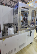
At this SEMICON China, Heyan Technology brought four exhibits, including a 12-inch dual-axis fully automatic dicing machine, a fully automatic cutting and sorting machine, a 12-inch fully automatic grinding and polishing machine, and a fully automatic film pouring machine.
Among them, the 12-inch dual-axis fully automatic dicing machine DS9261 is specially designed for the multi-size wafer dicing process in the semiconductor packaging process. Different from the traditional cutting dicing machine, this equipment innovatively realizes the precise half-cutting of ultra-thin wafers. This product is mainly used for the cutting of NAND chips and DRAM chips. It can realize high-precision half-cutting of wafers and non-contact handling of film-free wafers after cutting. The maximum cutting depth can be guaranteed to be ±7μm, which can meet the processing requirements of wafers with the thinnest thickness of 50μm. In addition, the equipment can also be used for film-free half-cutting of high-gram stacking processes, and can be used for processes such as stacking sheet slotting stress release. It is worth mentioning that Heyan Technology has a rich variety of product types for different customers to choose from. The general version of the 12-inch dual-axis fully automatic dicing machine is Heyan Technology's trump product, suitable for COWOS packaging customers. The upgraded version of the 12-inch dual-axis fully automatic dicing machine for the Triming process is provided to FAB factories. It has been successfully introduced to well-known domestic packaging manufacturers and has been unanimously recognized by customers.


1744127186029.png
The 12-inch fully automatic grinding and polishing machine on display is a fully automatic grinding machine with three axes, four grinding plates, automatic wafer transmission and loading and unloading. It is equipped with a high-power and high-rigidity air-floating spindle, a four-axis clean room-specific manipulator, a large-range high-resolution thickness gauge, etc. The machine is compatible with the back grinding of two mainstream wafers, 8/12 inches, and can realize automatic size switching without hardware replacement. In addition, the equipment also has high-precision grinding capabilities and intelligent control systems, which can effectively improve wafer grinding efficiency and quality stability, and is widely used in key processes such as wafer thinning and back grinding in semiconductor manufacturing. According to Heyan Technology, the equipment has been certified by a major domestic packaging and testing manufacturer and has received repeat purchase orders. This cooperation not only demonstrates Heyan Technology's outstanding technical strength and market competitiveness in the field of semiconductor equipment, but also lays a solid foundation for its continued development in the semiconductor industry. At the same time, it also provides a strong guarantee for customers' capacity expansion and technological innovation.

1744127256612.png

Please, Log in or Register to view URLs content!
 

tokenanalyst

Brigadier
Registered Member

North China Huachuang: Q1 net profit is expected to increase by 24.69%-52.79% year-on-year​

North Huachuang released its performance forecast, saying that the company expects to achieve operating income of 7.34 billion yuan to 8.98 billion yuan in the first quarter of 2025, a year-on-year increase of 23.35% to 50.91%; net profit attributable to shareholders of listed companies is 1.42 billion yuan to 1.74 billion yuan, a year-on-year increase of 24.69% to 52.79%; net profit after deducting non-recurring gains and losses is 1.4 billion yuan to 1.72 billion yuan, a year-on-year increase of 29.06% to 58.56%; basic earnings per share is 2.66 yuan/share to 3.26 yuan/share.
It further stated that during the reporting period, the company's integrated circuit equipment field, capacitive coupled plasma etching equipment (CCP), atomic layer deposition equipment (ALD), high-end single-wafer cleaning machine and other new products achieved key technological breakthroughs, process coverage increased significantly, and the market share of many mature products increased steadily. With excellent products, technology and service advantages, the company's market share continued to expand and operating income increased year-on-year.
North Huachuang said that as the company's revenue scale continues to expand, the scale effect has gradually emerged and the cost-to-income ratio has steadily declined, allowing the net profit attributable to shareholders of the listed company to maintain year-on-year growth.

Please, Log in or Register to view URLs content!
 

bd popeye

The Last Jedi
VIP Professional

Please, Log in or Register to view URLs content!

Please, Log in or Register to view URLs content!


A staff member displays a smart educational system at Guangzhou Shiyuan Electronic Technology Company Limited in Guangzhou, south China's Guangdong Province, March 20, 2025.

The city of Guangzhou has scaled up efforts to boost the growth of its semiconductor and integrated circuit industry. A whole industrial chain composed mainly of design, manufacturing, packaging and testing has gradually been built.

Statistics show that the city's integrated circuit industry saw a year-on-year increase of 25.8 percent in added value of industries above a designated size in 2024, with the output of analog chips and integrated circuit wafers up 23.7 percent and 68.9 percent year on year respectively. (Xinhua/Deng Hua)

Please, Log in or Register to view URLs content!


A staff member briefs on AI-powered teaching at Guangzhou Shiyuan Electronic Technology Company Limited in Guangzhou, south China's Guangdong Province, March 20, 2025. (Xinhua/Deng Hua)

Please, Log in or Register to view URLs content!


This photo shows a wafer at CanSemi Technology Inc. in Guangzhou, south China's Guangdong Province, March 20, 2025. (Xinhua/Deng Hua)

Please, Log in or Register to view URLs content!


This undated file photo shows a workshop of CanSemi Technology Inc. in Guangzhou, south China's Guangdong Province. (Xinhua)

Please, Log in or Register to view URLs content!


This photo shows mass flow controllers at Aosong Electronic Co., Ltd. in Guangzhou, south China's Guangdong Province, March 20, 2025. (Xinhua/Deng Hua)

Please, Log in or Register to view URLs content!
 

tokenanalyst

Brigadier
Registered Member

With a total investment of about 500 million yuan, Ruibao's high-end semiconductor equipment vacuum detection instrument and sensor project was put into use in June​

According to Chengdu Hi-Tech, Ruibao's high-end semiconductor equipment vacuum detection instrument and sensor R&D and production base is expected to be put into use in June this year, and a large number of headquarters base construction projects in Chengdu Future Science and Technology City are accelerating. The Ruibao high-end semiconductor equipment vacuum detection instrument and sensor R&D and production base project has a total construction area of about 48,000 square meters and a total investment of about 500 million yuan. The project mainly builds a high-end semiconductor equipment vacuum detection instrument and sensor R&D and production base.

The project consists of five major areas, among which Building 1 and Building 2 are R&D Building AB Area, Building 3 is the production plant, Building 4 is the process building, and Building 5 is the dormitory. The industrial park mainly produces vacuum detection instruments, helium mass spectrometer leak detectors, vacuum regulators and other products used in semiconductor, new energy, aerospace and other industries. At the same time, a professional national vacuum laboratory and testing center will be built to promote industrial development and technological innovation.

On November 19, 2024, Building 3 of Ruibao Science and Technology Industrial Park was officially capped. According to the news from Chengdu Future Science and Technology City in January 2025, Building 2 of Ruibao Science and Technology Industrial Park was capped recently.

Chengdu Ruibao Electronic Technology Co., Ltd. (abbreviated as: Ruibao Technology) is a professional supplier of vacuum detection products and technical solutions. With more than 20 years of experience in the field of vacuum detection, its business covers vacuum measurement, mass spectrometry leak detection, flow control, etc. Its products are widely used in scientific research institutes, solar energy, semiconductors, metallurgy, vacuum coating, refrigeration, pharmaceuticals, food and other fields. In recent years, the company has continued to increase its investment in technological innovation, and its products have successfully entered the first-tier semiconductor Fab and equipment manufacturers.

Please, Log in or Register to view URLs content!
 

tokenanalyst

Brigadier
Registered Member

Aixin Yuanzhi completed a strategic round of financing of over 1 billion yuan, further consolidating its leading position in the industry.​


Recently, Aixin Yuanzhi, a leading company in the field of artificial intelligence perception and edge computing chips, officially announced that it has successfully completed its C round of financing, with a financing amount of more than 1 billion yuan, which is one of the largest financing events in the domestic chip field in 2024. Investors in this round of financing include Ningbo Tongshang Fund, Zhenhai Industrial Investment, Chongqing Industrial Investment Fund, Chongqing Liangjiang Fund, Yuanhe Puhua, Weihao Chuangxin and other well-known investment institutions.

This round of funds will be mainly used to promote the technological research and development of the next generation of advanced artificial intelligence chips, accelerate the mass production of smart products, and increase market promotion efforts, aiming to provide customers with more efficient and intelligent solutions.

Since its establishment, Aixin Yuanzhi has completed several rounds of financing, with investors including Weihao Chuangxin, Qiming Venture Partners, Yingbai Capital, Meituan, Yuanhe Puhua, Tencent Investment and other well-known institutions. In the future, Aixin Yuanzhi will work closely with new and old shareholders, coordinate strategic resources, and jointly devote themselves to the exploration and development of automotive intelligence, edge computing and robotics.

Dr. Qiu Xiaoshen, founder and chairman of Aixin Yuanzhi, said: "I would like to thank investors for their support for Aixin Yuanzhi. It is your foresight and help that have enabled Aixin to continue to make breakthroughs in the field of artificial intelligence chips and inject strong impetus into industry innovation. Currently, AI is profoundly reshaping thousands of industries, and chips are the cornerstone of this change. Since its establishment, Aixin Yuanzhi has continued to focus on the research and development and mass production of edge-side artificial intelligence chips, and is committed to promoting the large-scale implementation of AI capabilities in different scenarios. In the future, we will continue to build the infrastructure of the intelligent era with our partners in an open and win-win attitude, and promote the sustainable development of the industry."​
 

tokenanalyst

Brigadier
Registered Member

SMIC applies for patent on semiconductor structure and its formation method to improve the electrical performance of semiconductor structure​

Information from the National Intellectual Property Administration shows that Semiconductor Manufacturing International Corporation (Shanghai) has applied for a patent titled "Semiconductor structure and method of forming the same", publication number CN 119767774 A, and the application date is September 2023.
The patent abstract shows a semiconductor structure and a method for forming the same, wherein a barrier layer is formed on the side wall of the first work function layer, and a second work function layer is formed on the side wall of the barrier layer. The barrier layer isolates the second work function layer from the first work function layer, and elements in the second work function layer are not easy to diffuse into the first work function layer through the barrier layer. Therefore, electrical parameter mismatch is not easy to occur between the first transistor and the second transistor. When the semiconductor structure is working, the first work function layer can well adjust the threshold voltage of the subsequently formed first transistor, and the second work function layer can well adjust the threshold voltage of the subsequently formed second transistor, which is beneficial to improving the electrical performance of the semiconductor structure.

1744212419121.png
 

tokenanalyst

Brigadier
Registered Member

Impact of chemical stochastics in extreme ultraviolet photoresists on the pattern quality​


Stochastic issues have been recognized as a major limiting factor in improving the pattern quality in extreme ultraviolet (EUV) lithography. These stochastic factors include photon shot noise (PSN) and chemical noise within the photoresist. While the impact of the former has been relatively well-established, the influence of the latter was largely unclear. Here, we apply high-throughput Monte Carlo simulations to investigate the chemical stochastics on pattern quality, focusing on the vertical photoacid generator (PAG) and base distribution and their aggregation. Our results indicate that the non-uniform vertical distribution of the PAG and base leads to the bottom residue. Suppressing the micro-aggregation of the PAG and base or limiting each aggregate containing 3 or fewer PAGs and 1 base (e.g., through chemical bonds) minimizes the negative impact of chemical stochastics on pattern quality. Increasing the dose and PAG concentration can effectively mitigate the negative impact of chemical stochastics on pattern quality, suggesting that PSN and chemical stochastics in EUV photoresist are intrinsically connected and need to be considered comprehensively. These findings serve as a valuable theoretical reference for the rational design of EUV photoresists.

Please, Log in or Register to view URLs content!
 
Top