Chinese semiconductor thread II

tokenanalyst

Brigadier
Registered Member

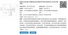
The Micro-Processing Equipment R&D Center Project of China Micro-Electronics Corporation was signed and settled in Nanchang High-tech Zone​


On April 7, the signing ceremony of the Micro-Processing Equipment R&D Center Project of China Micro-Semiconductor Equipment (Shanghai) Co., Ltd. (hereinafter referred to as "China Micro") was held. Li Hongjun, member of the Standing Committee of the Provincial Party Committee, Secretary of the Nanchang Municipal Party Committee, and Secretary of the Party Working Committee of Ganjiang New District, attended and witnessed the signing. Mayor Gao Shiwen and Chairman Yin Zhiyao of China Micro-Semiconductor delivered speeches respectively. Zhao Jie, member of the Standing Committee of the Municipal Party Committee and Secretary General of the Municipal Party Committee, An Baojun, member of the Standing Committee of the Municipal Party Committee and Deputy Mayor, Ma Yuzhou, member of the Standing Committee of the Municipal Party Committee and Deputy Mayor, and others attended.

Gao Shiwen pointed out in his speech that in recent years, Nanchang has insisted on building a city based on manufacturing, deeply implemented the "8810" action plan, and made every effort to build an electronic information industry cluster dominated by mobile smart terminals and LEDs, and promoted the electronic information industry to achieve "new" and transformation. As a benchmark enterprise in China's semiconductor equipment field, AMEC has been deeply engaged in the field of high-end micro-processing equipment for many years, and has been widely recognized by the market, ranking among the top in the global semiconductor equipment supplier rankings. The signing of this project is not only AMEC's high recognition of Nanchang, a hotbed of innovation and fertile ground for entrepreneurship, but will also inject stronger momentum into the development of Nanchang's advanced manufacturing industry and new quality productivity. Nanchang City will continue to be a "gold medal waiter" with heart and a "chief waiter" with affection, and fully support AMEC and its suppliers and customers to invest and start businesses in Chang to become bigger and stronger. AMEC is expected to continue to pay attention to Nanchang, support Nanchang, and cultivate Nanchang, combining its advantages in capital, technology, management, and brand with the development of Nanchang, promoting cooperation between the two sides in more fields and at a deeper level, and jointly create a new situation of mutual benefit and win-win.

Please, Log in or Register to view URLs content!
 

tokenanalyst

Brigadier
Registered Member

Sub-10-nm Lithography for Sn4–Oxo Clusters: Effect of Molecular Polarity on Sensitivity and Resolution​


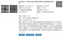
Tin-based metal–oxo clusters have recently garnered considerable attention in high-energy irradiation lithography because of their nanoscale patterning capabilities. However, achieving sub-10 nm resolution remains a challenge due to uncontrolled latent image gradients after exposure. In this study, the development mechanism of the Sn4–oxo cluster is investigated using a molecular polarity index model. Resolutions of 8 and 17 nm are successfully achieved for Sn4-TF using electron beam lithography (EBL) and extreme ultraviolet lithography (EUVL), respectively. A novel ultraviolet pre-irradiation modification strategy is proposed to enhance sensitivity by one-third for both EBL and EUVL. The experimental findings and theoretical analysis demonstrate that deep ultraviolet (DUV) lithography primarily degrades organic ligands and promotes Sn–O–Sn crosslinking, whereas EBL and EUVL drive both Sn–O–Sn and hydrocarbon crosslinking among Sn4–oxo clusters. This study deepens our understanding of Sn–oxo cluster photolithographic reaction mechanisms, offering critical insights for optimizing developers and enhancing resolution and sensitivity. These findings are expected to aid the realization of sub-10 nm node technology.

Please, Log in or Register to view URLs content!
 

tokenanalyst

Brigadier
Registered Member

Fast lithographic thick-mask model using overlapped patch matching​

Abstract​

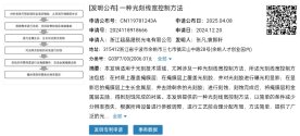
Modeling thick-mask effects is essential for lithography simulation at advanced technology nodes. This paper proposes a fast and accurate learning-based thick-mask model, dubbed as the fast diffraction transfer matrix (F-DTM) model, to solve this problem in deep ultraviolet lithography. The proposed method decomposes the whole mask pattern into overlapped patches. A set of diffraction transfer matrices (DTMs) is pre-calibrated, mapping the mask patches of different geometric features to the corresponding thick-mask diffraction near-fields. The overlapping decomposition can effectively alleviate the crack effects along the decomposition boundaries, thus reducing the model errors. Additionally, an acceleration technique is proposed to greatly improve the computational efficiency of DTMs, breaking through the speed bottleneck for model calibration. The results show that the proposed methods can effectively improve the calculation accuracy and efficiency compared to the traditional thick-mask models used extensively.

Please, Log in or Register to view URLs content!
 

tokenanalyst

Brigadier
Registered Member

Yongxiang Energy Technology Silane Gas Project Successfully Delivered​


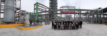
After several months of hard work, the EPC unit with an annual output of 1,500 tons of silane gas undertaken by our company for Yongxiang Energy Technology Co., Ltd., a subsidiary of Tongwei Group, was successfully delivered.
1744063603618.png

As a gas source for transporting silicon components, silane gas has become an important special gas that cannot be replaced by many other silicon sources because of its high purity and ability to achieve fine control. Domestic silane gas is mainly used for the preparation of silicon nitride anti-reflection film in solar cells, silicon nitride insulating protective film and amorphous silicon layer film in panel display, epitaxial silicon deposition, silicon oxide film deposition and silicon nitride film deposition in integrated circuits. It is one of the very important special gases in the panel display and semiconductor industries.

In recent years, new application fields of silane gas have continued to emerge, especially in the silicon-based negative electrode material industry. Silicon-based negative electrode materials have the advantages of high theoretical capacity, high initial charge and discharge efficiency, and low process cost, and are an important development direction for the next generation of negative electrode materials. After intensive pre-startup work deployment, Yongxiang Energy Technology Company's 1,500-ton silane gas project was successfully started up with one-time feeding.

Please, Log in or Register to view URLs content!
 

tokenanalyst

Brigadier
Registered Member
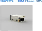
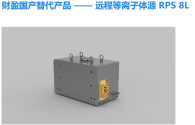
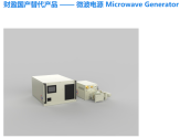
This Caiwin company started as a repair company of US and Japan equipment electrical components, now has launched a full fledge domestic line of semiconductor equipment components for ALD, CVD, PECVD, PVD, Etching and so on. The pressure for more domestic components, subsystems and material continues on.


1744066319434.png1744066358535.png
1744066393442.png1744066430617.png

Sanghai Caiying Semiconductor Co., Ltd. is a national high-tech enterprise specializing in technical services, R&D, and sales of semiconductor electronic control components. RF power supplies, matchers, RPS and other electronic control components are the key core components that "choke" semiconductor equipment. Caiying has an experienced R&D team in the field of semiconductor equipment electronic control. The independently developed RF, microwave, RPS and other electronic control products have broken the foreign technology monopoly in many aspects and completed in-situ replacement. It provides stable and reliable localization solutions for core components of equipment such as thin film deposition, etching, and cleaning.​

Please, Log in or Register to view URLs content!
 
Top