You are using an out of date browser. It may not display this or other websites correctly.
You should upgrade or use an alternative browser.
You should upgrade or use an alternative browser.
Chinese semiconductor thread II
- Thread starter vincent
- Start date
~40%I want to ask 1 question. As fyr 2025 what is the percentage of domestic SME utilization in China semicon manufacturing?
That is a good development~40%
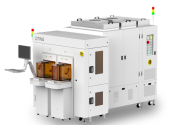
Qingting Optoelectronics 2D+3D advanced packaging volume inspection equipment shipped to leading domestic packaging and testing customers
QT successfully shipped the wafer-level 2D+3D mass inspection equipment Spectra-Wafer to a leading domestic packaging and testing customer. This milestone delivery demonstrates QT's deep technical accumulation in the field of advanced packaging, and also marks that the product has been successfully recognized by leading customers.
In the context of the complex and ever-changing global market environment, Qingting Optoelectronics insists on technological innovation as the core driving force and is committed to providing customers with domestic alternative products that are comparable to and surpass imported equipment. The Spectra-Wafer equipment delivered this time integrates high-speed, high-precision 2D+3D systems and AI intelligence and other technical features, representing the first-line level in the industry, and the product performance has established a good reputation among a series of leading customers.

Spectra-Wafer Product Highlights
Based on the self-developed 3D optical system and AI intelligent algorithm, the Spectra series of 2D+3D mass inspection equipment launched by Qingting Optoelectronics fully leverages the synergy advantages of optomechanical, electrical, software and computing, and better provides more advanced inspection equipment and strong technical support for the mass production inspection of WLP and 2.5D/3D mid-bump.
2D Vision System: Equipped with AI2.0 Detection Network
Spectra-Wafer's 2D vision system is equipped with a high-speed, large-surface, low-noise industrial camera and a high-power lighting system to accurately capture tiny defects. At the same time, the application of AI2.0 deep neural network technology has greatly reduced the demand for a large number of defect samples in traditional AI recognition networks, and can be quickly put online and greatly improve the recognition and classification accuracy and efficiency of complex defects.
3D Vision System: High-speed and high-precision 3D measurement
Spectra-Wafer's 3D vision system is equipped with an exclusive self-developed high-speed and high-precision 3D measurement module, which is deeply optimized for 3D imaging of bumping, surpassing the technical indicators of imported equipment of the same model, and providing reliable guarantee for the measurement of key parameters in advanced packaging.

Comprehensive testing capabilities
With full function coverage, it can accurately identify scratches, dirt, bubbles, cracks, measure key parameters such as bump height and bump coplanarity, and provide all-round and high-precision detection support for quality control of advanced packaging processes.
With the end of Moore's Law and the strong rise in demand for computing chips such as GPU and HBM, a new generation of 2.5D/3D advanced packaging technology represented by the COWOS process has emerged. Advanced packaging has entered the era of three-dimensional stacking, and 3D detection of interconnected bumps between wafers is crucial. An abnormal bump may cause the failure of an expensive chipset, and the number of bumps on each wafer often exceeds millions or even tens of millions. The Spectra series of equipment from Qingting Optoelectronics has solved a series of technical problems related to 3D wafer quantity detection, taking a solid step towards domestic substitution of such equipment.
Peking University's pioneered "subverting traditional crystal manufacturing methods"
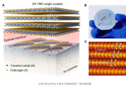
As the global silicon-based integrated circuit industry enters the "post-Moore era", chip performance improvement faces huge challenges. The team led by Liu Kaihui of Peking University overturned the traditional crystal manufacturing method and pioneered a new paradigm of "lattice mass transfer-interface growth", which for the first time realized the universal preparation of rhombohedral phase 3R-TMDs single crystals with controllable layer number and stacking structure.
The research team fully dissolved the chalcogenide elements into the alloy substrate in the form of single-atom supply. The reactive atoms continuously transferred mass in the metal lattice through the concentration and chemical potential gradient, and epitaxially precipitated a new layer at the interface between the substrate and TMDs. By continuously "lifting" the formation layer, the crystal grows upward like a "bamboo shoot", driven by its own structure, completely subverting the traditional crystal growth model.

This innovative method has three major advantages: ensuring the rapid growth and uniform arrangement of the crystal structure; effectively avoiding the accumulation of defects; and increasing the purity of various two-dimensional materials such as graphite and molybdenum sulfide by 10-100 times, greatly improving the controllability of the crystal structure.
This major achievement, known as a "new paradigm for preparing biologically grown crystals," has laid a solid foundation for the research and development of the next generation of high-performance electronic and photonic chips.
The research team fully dissolved the chalcogenide elements into the alloy substrate in the form of single-atom supply. The reactive atoms continuously transferred mass in the metal lattice through the concentration and chemical potential gradient, and epitaxially precipitated a new layer at the interface between the substrate and TMDs. By continuously "lifting" the formation layer, the crystal grows upward like a "bamboo shoot", driven by its own structure, completely subverting the traditional crystal growth model.

This innovative method has three major advantages: ensuring the rapid growth and uniform arrangement of the crystal structure; effectively avoiding the accumulation of defects; and increasing the purity of various two-dimensional materials such as graphite and molybdenum sulfide by 10-100 times, greatly improving the controllability of the crystal structure.
This major achievement, known as a "new paradigm for preparing biologically grown crystals," has laid a solid foundation for the research and development of the next generation of high-performance electronic and photonic chips.
Total investment of 500 million yuan! Silicon State Semiconductor IC packaging and testing manufacturing project signed
On March 27, a signing ceremony was held for the commissioning of the Silicon State Semiconductor Integrated Circuit Packaging and Testing Manufacturing Project in Huishan Economic Development Zone.
Silicon State Semiconductor, which has been deeply involved in the semiconductor packaging and testing track for ten years, has built a "packaging and testing technology chain" covering the entire process from wafer testing to module assembly. With the "double certification" qualifications of national high-tech enterprises and provincial specialization, relying on import and export qualifications and public service platforms, engineering research centers, and corporate technology centers, with "50+" core technology patents and "200+" corporate service performance, it continues to lead the packaging and testing track and establish a leading position in industry technology.
"Wuxi is one of the gathering places for enterprises in the integrated circuit industry, and Huishan Economic Development Zone has done a lot of work in enterprise services and factor guarantee, which is an important reason for our determination to settle down." Mu Yunfei, chairman of Silicon State Semiconductor, said that the project plans to invest a total of more than 500 million yuan, with a layout of more than 17,000 square meters of R&D and manufacturing bases, and will create a "design verification + process optimization + mass production service" three-in-one packaging and testing innovation platform to form a strong radiation driving effect. At present, the project has completed industrial and commercial registration and team formation, and is scheduled to be put into production this month. After reaching full production, the annual invoiced sales will exceed 500 million yuan, and the annual tax payment will reach 25 million yuan.
Where can I read the review about the Japanese semi?Hyundai Motor Securities in Korea has just dropped several shocking pieces of news.
Review of Japanese and Taiwanese companies
Chinese Foundry Companies Entering the Market with 6 New Companies in addition to the Existing 3 / SMIC's 5mm Products to be Produced by Huawei, Sicarrier
Mass production through collaboration
5nm products are likely to be installed in Huawei's new inference chip, Ascend 910C/This product may also be installed in HBM2e, etc.
CXMT succeeded in developing the 15nm process and started mass production of LPDDRS products, etc. CXMT prepares for mass production of HBM3e in 2027
YMTC plans to enter the DRAM market through mass production of LPDDR5 products in 2026
A new DRAM company other than CXMT is expected to emerge in China
Deepseek, self-driving cars, robotics, and foldable smartphones are all being completed at a level that far exceeds market expectations, and the growth of Chinese semiconductor companies is also exceeding market expectations. In particular, Chinese foundry companies have all built 12-inch fabs with a monthly capacity of 10K-60K due to the difficulty in securing 8-inch equipment amid the continuous establishment of new companies. Since products that would be made on an 8-inch scale are being made on a 12-inch scale, they are being supplied at a 20-30% discount compared to Taiwanese and Korean industries. In the case of Korean and Taiwanese 8-inch foundry companies, even if they turn a profit due to low depreciation expenses, it seems inevitable that they will incur an EBITDA deficit in the near future. In addition, SMIC is mass-producing 7nm products on the N+2 process using DUV, and recently it is making 5mm products through a +3 plant. Of course, since they are making 5mm with DUV, not EUV, the defect rate is high, and the eastern part has a negative effect on price competitiveness, but they are offsetting this with government subsidies, so China's move cannot be taken lightly. It appears that 5mm products are being produced through collaboration with equipment companies called SMIC, Huawei Hisilicon, and Sicamer.
SMIC's 7nm Capa is estimated at 10K per month, and Som Capa at 5K per month. The amount of semiconductors supplied is also limited due to low cost. The main products are understood to be Kirin 90005 supplied to Huawei smartphones and Ascend 910B, an inference semiconductor. In particular, Ascend 910B was used as DeepSeek's inference service chip. Meanwhile, it seems that it will be applied to the 5m Ascend 910C, which is currently being ramped up. There are rumors that Ascend 910C will be equipped with HBM2. This is because it is difficult to secure HBM3 due to US sanctions.
However, since Chinese DRAM companies are developing HBM3 and HBM2, it seems that Chinese HBM will be mounted on the Hanwei Ascend Series within the next 2-3 years. Currently, Chinese DRAM companies are rapidly encroaching on the market centered on LPDDR4 by CXMT. It is estimated that 85% of CXMT's production is LPDDR4, and Korean DRAM companies are rapidly leaving the LP DDR4 market. CXMT is currently known to have succeeded in developing a 15cm process and is producing LPDDR5 (16Gb) and PC DDR5 (16Gb) products, and is planning to mass produce HBM3 in 2026 and HBM3 in 2027. Of course, even if CXMT mass-produces HBM, the possibility of Chinese HBM being mounted on AI Servers, where information security issues are important, is slim. In addition, due to US sanctions, Korean companies are unable to directly supply HBM3 to China. Given that Chinese companies are indirectly supplying HBM to NVIDIA H20, the impact of Chinese companies’ mass production on Korean companies is expected to be minimal. Meanwhile, during our visit to Taiwan Supply Chain, we were able to confirm companies in China that are preparing to enter the DRAM market for the first time. For example, YMTC, which succeeded in mass producing 294 layers in the 3D NAND market through its unique technology called Xtacking, is preparing to enter the DRAM market. YMTC is understood to be planning to mass produce LPDDR5 products in 2006. In particular, although XMC, a subsidiary of YMTC, is a foundry company, it is likely that YMTC will enter the HBM market in the future as it has good TSV technology.
View attachment 149119
Where can I read the review about the Japanese semi?
