Chinese semiconductor thread II

tokenanalyst

Brigadier
Registered Member

10 integrated circuit projects settled in Optics Valley, covering the entire industry chain​


According to the official microblog of China Optics Valley, the "Core Gathering in Jiangcheng, Smart Wuhan" Wuhan Integrated Circuit Industry Business Matchmaking Conference was held in Optics Valley a few days ago. At the scene, 10 key projects including Wuhan Integrated Circuit Technology and Industry Promotion Center, Juxinwei Integrated Circuit Design Project, Weichong Semiconductor Integrated Circuit Measurement Equipment Project, and Integrated Circuit Precision Mounting Equipment Project were signed and settled in Optics Valley, covering the entire industrial chain of "chip design-wafer manufacturing-packaging and testing-equipment and materials", which will further strengthen the integrated circuit industry ecology of Optics Valley.
Among them, the Wuhan Integrated Circuit Technology and Industry Promotion Center is jointly built by Wuhan City, East Lake High-tech Zone and China Information and Communications Technology Group. It will provide EDA/IP resource sharing, design, wafer fabrication, packaging and other services to semiconductor companies in Wuhan and even the whole country, drive the construction of the local semiconductor industry ecosystem, and create a national leading semiconductor service platform. It is expected to open in the second quarter of this year.
It is understood that Optics Valley is planning to build a 7 square kilometer memory industry innovation district and a 14 square kilometer compound semiconductor industry innovation district. Focusing on the core technology research and development, product tape-out, talent introduction and cultivation, and scene supply of integrated circuit enterprises, a systematic and inclusive policy has been formulated to support enterprise development throughout the entire cycle, especially supporting enterprise innovation according to the high proportion of project research and development and tape-out costs, and supporting enterprises to introduce leading talents with a maximum of 100 million yuan.
In addition, Optics Valley will also establish the Optics Valley High-Quality Development Fund, adding a new parent-child fund cluster covering the entire life cycle of angel funds, venture capital, mergers and acquisitions, etc., with a focus on investing in optoelectronic information industries such as integrated circuits.

Please, Log in or Register to view URLs content!
 

tokenanalyst

Brigadier
Registered Member

Nano Semiconductor accelerates DFI product track sprint​

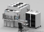
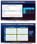
On March 27 , Hefei Nano Semiconductor Co., Ltd. successfully held a 7nm advanced process wafer defect detection product launch conference at the Kerry Hotel Pudong, Shanghai during SEMICON 2025. In the early stage of the conference, target customers and semiconductor industry investment institutions were invited to witness the entire development process of Nano Semiconductor's DFI-70/80/90 product upgrades and iterations.

The two graphic wafer dark field defect inspection equipment launched at the conference are DFI-70 (performance benchmark PUMA 9980 ), which is suitable for 2Xnm process and DFI-80 (performance benchmark Voyager 1015 ), which is suitable for 1Xnm and 7nm and below more advanced process.
Currently, one DFI-70 and one DFI-80 have been tested and are ready for shipment. The mature application of DFI-70/80 will accelerate the development of DFI-90 (performance benchmark Voyager 1035 ) products.

1743552759915.png

In the field of chip mass production ( HVM ), DFI products solve two key challenges for yield improvement, equipment and process monitoring for logic and memory components at advanced technology nodes. The DFI-70 and DFI-80 systems provide industry-leading new technologies for defect detection of graphic wafers, including the use of deep ultraviolet DUV laser light sources, three-channel signal acquisition and high-efficiency quantum sensors, as well as unique control of power density. They perform non-destructive testing of sensitive and delicate photoresists at many key nodes of the chip manufacturing process, especially after development ( ADI ), filling the gap in domestic equipment for defect detection of 14nm and more advanced process processes .

Nano Semiconductor, a high-tech enterprise focusing on the research and development of advanced process wafer defect detection equipment, is working with its wholly-owned subsidiary SemiX to make a full sprint in the race of domestic substitution of independently developed wafer defect detection products. The company adheres to the concept of "independent innovation and technological breakthroughs" and insists on and attaches great importance to the independent design and development of product technology. At present, the DFI equipment developed by Nano Semiconductor has a domestic substitution rate of 90% for core components, achieving independent control and providing a guarantee for the subsequent upgrade and optimization of DFI products.​

Please, Log in or Register to view URLs content!
 

tokenanalyst

Brigadier
Registered Member

Maxsun Technology: Multiple equipment in the field of semiconductor packaging have been localized​


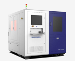
Recently, Maxsun Technology Co., Ltd. said in response to investors' questions that in the field of semiconductor packaging, Maxsun Technology Co., Ltd. insists on R&D and innovation, based on the integrated strategic layout of "core components, key consumables, high-end equipment, and advanced technology", and has achieved the localization of multiple equipment for grinding and bonding processes, ensuring and improving the quality, yield and production efficiency of client packaging products. Recently, the company has demonstrated a complete set of process equipment solutions for 3D packaging, including wafer thinning, laser grooving and hybrid bonding; at the same time, for ultra-thin memory processing, the company has launched a full process solution (covering laser modification and cutting equipment, integrated grinding and polishing equipment and wafer expansion equipment). Among them, the company's independently developed first domestic dry-polishing wafer integrated grinding and polishing equipment has made key progress, and the process verification on the client side has entered the final stage and will soon be mass-produced. For operating data, please pay attention to the relevant announcements disclosed by the company on the information disclosure website designated by the China Securities Regulatory Commission.

1743605122673.png

Please, Log in or Register to view URLs content!
 

tokenanalyst

Brigadier
Registered Member

Significant progress has been made in the manufacturing and measurement of EUV lithography light source collection mirrors​

To filter out infrared light from the driving light source in the extreme ultraviolet lithography (EUVL) light source system, a rectangular grating structure needs to be fabricated on the surface of the collection mirror. However, the collection mirror grating usually undergoes deformation during the manufacturing process, resulting in a decrease in filtering efficiency. The process errors of grating height and upper base angle need to be controlled within ± 13nm and 0.016 °, respectively, which puts extremely high demands on the measurement method. This article proposes a fast and non-destructive measurement method for collecting mirror grating deformation structures to meet their extreme manufacturing requirements.
At present, the most advanced commercial EUV lithography machines use laser generated plasma light source systems. In this system, a driving laser from the infrared (IR) band strikes the droplet tin target twice, causing complete ionization and generating EUV radiation. After being collected and reflected by the collection mirror, EUV radiation is focused onto the central focal point to enter the subsequent optical system.
However, in the process of collecting and focusing EUV, IR light from the driving laser is usually introduced. The energy of IR light is extremely high and will propagate along the entire EUV lithography system until it reaches the surface of the wafer. This not only causes damage to optical components, but also results in severe optical distortion and decreased pattern accuracy in the final lithography pattern. In order to filter out IR, a rectangular grating needs to be fabricated on the collection mirror substrate to diffract IR from the 0th order to higher orders, and a diaphragm is used to block the high-order diffracted light, as shown in Figure 1 (a). However, rectangular shapes are prone to deformation during the manufacturing process, resulting in asymmetric trapezoidal structures, as shown in Figure 1 (b), which reduces the infrared filtering capability of the grating. Therefore, it is necessary to analyze the deformation structure of the collection mirror grating to determine its tolerance range, and establish a model to achieve fast and accurate non-destructive measurement.
1743609098446.pngMeasurement model of EUV collection mirror grating deformation structure (core content of the article)
Recently, Lin Nan's team from the Chinese Academy of Sciences Shanghai Institute of Optics and Mechanics proposed a fast and accurate nondestructive measurement method for the deformed structure of EUV collecting mirror grating. The article first establishes an efficient and accurate scalar diffraction model for collecting deformation analysis of mirror gratings, targeting the deformation structure of gratings. Secondly, propose a two-step measurement method. The first step is to quickly screen whether the key dimension parameters of the grating meet the tolerance requirements; The second step is to quantitatively reconstruct the size parameters of the gratings selected as unqualified. This method provides a new solution for the inverse scattering problem in collecting mirror grating measurements. It does not require complex numerical calculations and dependence on large datasets, while still providing accurate measurement results, which is beneficial for achieving online non-destructive measurement of collecting mirror grating structures.

The results were published in Optics and Lasers in Engineering (Yunyi Chen, Zexu Liu, Nan Lin. Computational metrology method of collector mirror for EUV lithography [J]. Optics and Lasers in Engineering 189 (2025) 108946).

A scalar diffraction model was established for the common deformation structure of the collection mirror grating (i.e., asymmetric trapezoidal structure) to achieve tolerance analysis in order to obtain a reflectance size with IR less than 0.2%. Compared to the vector diffraction method, this model has a computational speed increase of nearly 5 orders of magnitude, and its normalized root mean square error is only on the order of 10-3. The analysis results indicate that the height and top tilt angle of the grating have a significant impact on the IR reflectivity, with a tolerance of ± 13 nm for height and only 0.016 ° for top angle.

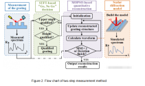
To meet the extreme measurement requirements of collecting mirror gratings, a two-step measurement model based on optical scattering method is proposed, as shown in Figure 2. This model reconstructs the zero order and ± one order of the grating as measurement signals. The first step is to establish a "Go, No Go" model based on short-time Fourier transform (STFT), and detect whether the key size parameters of the grating meet the tolerance requirements by analyzing the spectral mutation positions and numbers in the time-frequency diagram. Qualified gratings will no longer undergo quantitative reconstruction, thereby reducing unnecessary calculations. Under the condition of a signal-to-noise ratio of 500:1, the model can achieve an accuracy of 91.3%, as shown in Figure 3 (a), and improve the overall model efficiency by at least one order of magnitude. In the second step, an improved multi-objective particle swarm optimization (MOPSO) model was further established for the detection of non-conforming gratings to achieve quantitative reconstruction of key dimensional parameters of the gratings. Under the same noise environment, the relative error of the reconstructed height of the model is only 0.19%, and the relative error of the vertex angle is only 0.84%, as shown in Figures 3 (b) and (c). The results fully meet the tolerance requirements of the collection mirror grating.
upload.html

1743609130536.png
Please, Log in or Register to view URLs content!
CIOMP EUV collector mirror

View attachment 148252
 

sunnymaxi

Major
Registered Member

Significant progress has been made in the manufacturing and measurement of EUV lithography light source collection mirrors​

To filter out infrared light from the driving light source in the extreme ultraviolet lithography (EUVL) light source system, a rectangular grating structure needs to be fabricated on the surface of the collection mirror. However, the collection mirror grating usually undergoes deformation during the manufacturing process, resulting in a decrease in filtering efficiency. The process errors of grating height and upper base angle need to be controlled within ± 13nm and 0.016 °, respectively, which puts extremely high demands on the measurement method. This article proposes a fast and non-destructive measurement method for collecting mirror grating deformation structures to meet their extreme manufacturing requirements.
At present, the most advanced commercial EUV lithography machines use laser generated plasma light source systems. In this system, a driving laser from the infrared (IR) band strikes the droplet tin target twice, causing complete ionization and generating EUV radiation. After being collected and reflected by the collection mirror, EUV radiation is focused onto the central focal point to enter the subsequent optical system.
However, in the process of collecting and focusing EUV, IR light from the driving laser is usually introduced. The energy of IR light is extremely high and will propagate along the entire EUV lithography system until it reaches the surface of the wafer. This not only causes damage to optical components, but also results in severe optical distortion and decreased pattern accuracy in the final lithography pattern. In order to filter out IR, a rectangular grating needs to be fabricated on the collection mirror substrate to diffract IR from the 0th order to higher orders, and a diaphragm is used to block the high-order diffracted light, as shown in Figure 1 (a). However, rectangular shapes are prone to deformation during the manufacturing process, resulting in asymmetric trapezoidal structures, as shown in Figure 1 (b), which reduces the infrared filtering capability of the grating. Therefore, it is necessary to analyze the deformation structure of the collection mirror grating to determine its tolerance range, and establish a model to achieve fast and accurate non-destructive measurement.
View attachment 149238Measurement model of EUV collection mirror grating deformation structure (core content of the article)
Recently, Lin Nan's team from the Chinese Academy of Sciences Shanghai Institute of Optics and Mechanics proposed a fast and accurate nondestructive measurement method for the deformed structure of EUV collecting mirror grating. The article first establishes an efficient and accurate scalar diffraction model for collecting deformation analysis of mirror gratings, targeting the deformation structure of gratings. Secondly, propose a two-step measurement method. The first step is to quickly screen whether the key dimension parameters of the grating meet the tolerance requirements; The second step is to quantitatively reconstruct the size parameters of the gratings selected as unqualified. This method provides a new solution for the inverse scattering problem in collecting mirror grating measurements. It does not require complex numerical calculations and dependence on large datasets, while still providing accurate measurement results, which is beneficial for achieving online non-destructive measurement of collecting mirror grating structures.

The results were published in Optics and Lasers in Engineering (Yunyi Chen, Zexu Liu, Nan Lin. Computational metrology method of collector mirror for EUV lithography [J]. Optics and Lasers in Engineering 189 (2025) 108946).

A scalar diffraction model was established for the common deformation structure of the collection mirror grating (i.e., asymmetric trapezoidal structure) to achieve tolerance analysis in order to obtain a reflectance size with IR less than 0.2%. Compared to the vector diffraction method, this model has a computational speed increase of nearly 5 orders of magnitude, and its normalized root mean square error is only on the order of 10-3. The analysis results indicate that the height and top tilt angle of the grating have a significant impact on the IR reflectivity, with a tolerance of ± 13 nm for height and only 0.016 ° for top angle.

To meet the extreme measurement requirements of collecting mirror gratings, a two-step measurement model based on optical scattering method is proposed, as shown in Figure 2. This model reconstructs the zero order and ± one order of the grating as measurement signals. The first step is to establish a "Go, No Go" model based on short-time Fourier transform (STFT), and detect whether the key size parameters of the grating meet the tolerance requirements by analyzing the spectral mutation positions and numbers in the time-frequency diagram. Qualified gratings will no longer undergo quantitative reconstruction, thereby reducing unnecessary calculations. Under the condition of a signal-to-noise ratio of 500:1, the model can achieve an accuracy of 91.3%, as shown in Figure 3 (a), and improve the overall model efficiency by at least one order of magnitude. In the second step, an improved multi-objective particle swarm optimization (MOPSO) model was further established for the detection of non-conforming gratings to achieve quantitative reconstruction of key dimensional parameters of the gratings. Under the same noise environment, the relative error of the reconstructed height of the model is only 0.19%, and the relative error of the vertex angle is only 0.84%, as shown in Figures 3 (b) and (c). The results fully meet the tolerance requirements of the collection mirror grating.
upload.html

View attachment 149239
Please, Log in or Register to view URLs content!
the surprise for me is, this ''EUV lithography light source collection mirrors'' project led by SIOMP alongside Precision optics department and Laser Laboratory of Shanghai.. this is different from CIOMP led high precision aspherical 4m ultra precision mirror. which took them 20 years to manufacture and conquered entire process..

so we have two different institutes working on this Ultra precision EUV component.. i like it
 

tokenanalyst

Brigadier
Registered Member

VeriSilicon Launches Next-Generation ISP9000 Image Signal Processor with Integrated AI to Enable Intelligent Vision Applications​

VeriSilicon (Visilicon, stock code: 688521.SH) today released its ISP9000 series image signal processor (ISP) IP - a new generation of AI ISP solutions designed for the growing demand for intelligent vision applications. The ISP9000 uses a flexible AI-optimized architecture, provides excellent image quality, has low-latency multi-sensor management capabilities, and is deeply integrated with AI, making it ideal for applications such as smart machines, surveillance cameras, and AI PCs.

With the AI-powered ISP function, VeriSilicon's ISP9000 series IP can achieve excellent image quality. It integrates advanced AI noise reduction (AI NR) algorithms, combined with multi-scale 2D and 3D noise suppression and YUV domain chrominance noise suppression (CNR), forming a multi-domain noise reduction architecture that can effectively reduce noise and retain details, especially in extremely low light environments. This series of IP supports triple-exposure high dynamic range (HDR) processing and dynamic range compression, and is equipped with a 20-bit pipeline to preserve key details in light and dark areas in high dynamic range scenes. In addition, the ISP9000 also integrates 3A functions, namely automatic exposure, autofocus, and automatic white balance, and supports up to 25 regions of interest (ROI) configurations, which can realize AI-assisted target detection and recognition. Users can also integrate third-party 3A libraries to flexibly customize 3A algorithms for specific application requirements.

ISP9000 supports multi-sensor configurations, and through hardware-accelerated multi-context management (MCM) and frame slicing processing mechanisms, it achieves efficient data stream switching, ensures the stability of multi-sensor data streams, and has the advantages of low latency and low cost. It supports up to 16 sensors and integrates VeriSilicon's VI200 video interface IP to achieve seamless connection with the mainstream MIPI Rx interface. The scalable multi-core architecture of ISP9000 supports high-performance processing up to 8K@30fps and 4K@120fps. Through VeriSilicon's FLEXA SBI interface, ISP9000 can optimize data transmission and efficiently connect video encoders, neural network processing units (NPUs) or display processors to form an optimized subsystem solution.

In addition, to further enhance the intelligent vision function, the ISP9000 is equipped with the VeriSilicon AcuityPercept AI automatic ISP tuning system. Unlike the traditional tuning method that focuses on human-perceived image quality, AcuityPercept optimizes the ISP settings to achieve high-quality target recognition performance in the AI/NPU path, which can adapt to specific AI algorithms and application requirements.

Please, Log in or Register to view URLs content!
 
Top