Chinese semiconductor thread II

sunnymaxi

Major
Registered Member
But nevertheless Sicarrier develop an insane array of tools in a very short time and complete China wafer processing gaps.
Sicarrier literally mentioned these tools are capable for 28nm-5nm nodes.. GAAFET mentioned too.

team announced, this is just the beginning. we will release more tools next year.

looks like they will announce Lithography too probably in next phase.
 

tokenanalyst

Brigadier
Registered Member

Technological breakthroughs and industrialization: Kaishitong leads the domestic ion implantation machine market


Kaishitong leads the industrialization of domestic integrated circuit ion implanters. The company has developed and mass-produced a series of products such as low-energy, large-beam ion implanters and high-energy ion implanters, filling the domestic gap. It is at the forefront of domestic production in terms of equipment installed capacity, performance and stability, and has achieved full coverage of various chip processes such as logic, storage, power, CIS image sensors, etc.

At this year's SEMICON China exhibition, Kaishitong brought a full range of integrated circuit ion implanter product matrix. Through long-term technical research and mass production applications, Kaishitong's ion implanter has been continuously upgraded and iterated in key technologies such as ion source, optical path system, wafer transfer, particle contamination control, and software automation. The key performance indicators have been continuously improved and have been widely recognized by wafer fab customers. Since the first order breakthrough in 2020, Kaishitong has received a total of nearly 60 orders for 12-inch integrated circuit ion implanter equipment, with a total order amount of more than 1.4 billion, of which more than 50% are repeat orders. It has completed the delivery of more than 40 production lines and achieved mass production, serving more than a dozen key chip manufacturing companies and national projects.

------------------------------------------------------
Under the global semiconductor industry competition pattern, the independent control of key materials and core equipment has become a national strategy. In recent years, Wanye Enterprise has made forward-looking layouts in the field of semiconductor equipment and components through the strategic path of "external expansion and mergers and acquisitions + industrial integration". Its subsidiary Kaishitong occupies an important position in the domestic integrated circuit ion implantation machine market.

As the controlling shareholder of Wanye Enterprise, Pioneer Technology Group leads the world in the production and sales of indium, gallium, germanium, selenium, tellurium, and bismuth metals. Its products are highly scarce and have great strategic significance. Especially in the field of semiconductor materials, Pioneer Technology has deep technical accumulation and upstream and downstream industrial resource advantages. It has a full industrial chain of high-end materials-devices-modules-systems-equipment covering the pan-semiconductor field, and has built a complete ecological closed loop from underlying materials to terminal applications. With Pioneer Technology's global leadership in the entire industrial chain of rare metals, a closed-loop layout of "materials + equipment + parts" has been created. In January this year, Wanye Enterprise, as the only platform in the Pioneer Technology system that focuses on the deep processing and operation of bismuth metal business, is fully promoting the product business of bismuth metal, injecting strong momentum into the sustainable development of Wanye Enterprise.
Please, Log in or Register to view URLs content!
 

tokenanalyst

Brigadier
Registered Member

ProPlus plans to acquire Ruichengxinwei, which is expected to constitute a major asset reorganization​

Prologis announced that the company is planning to purchase the controlling stake of Chengdu Ruichengxinwei Technology Co., Ltd. (hereinafter referred to as "Ruichengxinwei") by issuing shares and paying cash, and at the same time intends to raise supporting funds. According to preliminary calculations, this transaction is expected to constitute a major asset reorganization and is expected to constitute an affiliated transaction. This transaction will not lead to a change in the company's actual controller and does not constitute a reorganization listing.

Ruichengxinwei was established in December 2011 with a registered capital of approximately 56.0929 million yuan. Its business scope includes research and development, sales of electronic components, computer hardware and software, electronic equipment, etc. Previously, Ruichengxinwei had attempted to be listed on the Shanghai Stock Exchange's Science and Technology Innovation Board, but on March 2, 2023, due to the withdrawal of its application for issuance and listing, the Shanghai Stock Exchange terminated Ruichengxinwei's Science and Technology Innovation Board issuance and listing review.


Prologix is an EDA listed company, whose main business includes providing EDA products and solutions to customers. In 2024, the company achieved total operating revenue of 420 million yuan, a year-on-year increase of 27.56%. Prologix said that the company is continuously upgrading and improving strategic products and developing new products based on the DTCO (design-process collaborative optimization) methodology, and continuously increasing R&D investment.
1743086346002.png

Please, Log in or Register to view URLs content!
 

tokenanalyst

Brigadier
Registered Member

New progress in Yinchuan's billion-level semiconductor-related project​


Recently, a 10 billion-level semiconductor industry-related project located in Yinchuan, Ningxia has also made new progress, namely, the high-temperature superconducting silicon single crystal equipment and crystal production project has officially broken ground.

It is understood that the project plans to invest 10 billion yuan and build high-temperature superconducting silicon single crystal growth equipment manufacturing and high-quality silicon crystal production projects in three phases. After the project is completed, it will reach an annual production capacity of 40,000 tons of high-quality single crystal silicon and 600 high-temperature superconducting photovoltaic-grade single crystal silicon growth equipment, forming a world-class high-end manufacturing of high-temperature superconducting magnetron silicon single crystal growth equipment and silicon single crystal production capacity. The first phase of the project is scheduled to start construction in the first quarter of this year. After reaching full production, it is expected to achieve an annual sales revenue of 3.5 billion yuan and create more than 1,000 jobs.

Please, Log in or Register to view URLs content!
 

tokenanalyst

Brigadier
Registered Member

A semiconductor intelligent manufacturing project involving silicon carbide with a total investment of 300 million yuan settled in Hubei​


On the morning of March 24, the People's Government of Yangxin County, Hubei Province and Jiangsu Zhuoyuan Semiconductor Co., Ltd. held a grand project signing ceremony in Rugao City, Jiangsu Province. The "Zhuoyuan Semiconductor Project" with a total investment of 300 million yuan was officially signed and settled in Yangxin Economic Development Zone.

According to the agreement, Jiangsu Zhuoyuan Semiconductor will establish a wholly-owned subsidiary in Yangxin, focusing on the research and development and manufacturing of third-generation semiconductor core equipment, covering MPCVD diamond growth equipment, silicon carbide growth systems and 12-inch large-diameter direct-pull silicon wafer growth equipment.

After the project reaches full production capacity, it will be able to form an annual production capacity of 100 MPCVD equipment, 10 silicon carbide equipment, and 5 large silicon wafer equipment, with an estimated annual output value of 200 million yuan, injecting core momentum into Yangxin's construction of a modern industrial system.


Zhuoyue Semiconductor will rely on its patent cluster advantages and independent controllable technology system in the field of third-generation semiconductor material preparation to help Yangxin build an innovation highland for the semiconductor industry in the middle reaches of the Yangtze River.

Please, Log in or Register to view URLs content!
 

tokenanalyst

Brigadier
Registered Member

Hwatsing expand its product matrix in SEMICON 2025​


Innovative product matrix leads to technological breakthroughs The content of Huahai Qingke's exhibition has attracted much attention from all walks of life. At the opening, consultants came in droves, the exhibition area was crowded with people, the atmosphere was warm, and everyone actively exchanged and discussed. The new products made a grand appearance and quickly became the focus of the audience, arousing in-depth discussions and gaining wide praise.

Universal-H300 The 12-inch CMP equipment adopts an innovative polishing system architecture and integrates advanced polishing technology, high efficiency and high stability.

Third-generation and a half CMP equipment Universal-TGS200 Equipped with three sets of polishing modules with innovative polishing system architecture and integrated back-end cleaning technology, it is a highly automated and efficient dedicated CMP equipment designed for third-generation semiconductor materials (SiC).

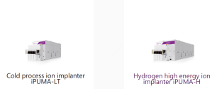
Large beam ion implanter IPUMA-LE It uses advanced beam climbing technology, integrates magnetic field and electric field modules, and is equipped with precise measurement technology. It is a large-beam ion implanter with excellent ion screening capabilities and accuracy.

Thin film polishing machine Versatile-GP300 The innovative layout of the new machine integrates advanced ultra-precision grinding, CMP and post-cleaning processes to meet the needs of ultra-precision wafer thinning technology in 3D IC manufacturing, advanced packaging and other fields.

Edge trimmer Versatile-DT300 The high-efficiency, high-cleanliness fully automatic dual-axis wafer edge trimming equipment can accurately solve the edge collapse problem during wafer thinning and improve the thinning quality. It can meet the technical requirements of manufacturing processes such as memory chips, image sensors, and advanced packaging.

Edge polishing machine Master-BN300 It integrates high-precision polishing, efficient cleaning and precise measurement functions to significantly improve the smoothness of the wafer edge, meet the technical requirements of high-precision edge processing in the semiconductor manufacturing field, and meet the technical requirements of key processes such as memory chips and advanced packaging.

Brush cleaning machine HSC-S3810 Equipped with an excellent parameter closed-loop control system, it has front, back and edge cleaning functions, and the advanced atomization cleaning technology can achieve damage-free cleaning.

Please, Log in or Register to view URLs content!
 

tokenanalyst

Brigadier
Registered Member

Flow pattern and wave propagation induced by local energy deposition at droplet surface​

Abstract​

Interaction between metallic droplets and picosecond laser pre-pulse can shape the droplet into a target more favorable for the main pulse to efficiently generate extreme ultraviolet (EUV) light for nanolithography. After the radiation of the pre-pulse, flow pattern and wave propagation in the droplet are responsible for the deformation and fragmentation of the droplet at a late time. In this study, we numerically investigate the acoustic response and dynamic behaviors of a droplet subjected to a localized heat pulse in the vicinity of the droplet surface, which models the energy deposition of a picosecond (ps) laser pre-pulse. A second-order conservative sharp interface method is adopted to simulate corresponding compressible inviscid two-phase flows. Based on the numerical results, we find that a wave structure of compression-expansion-compression waves propagates in the spherical droplet, and that the asymmetry of the heat source around the droplet surface accounts for the occurrence of the secondary compression wave. Then, we assess the occurrence and propagation of the wave structures, and correlate the wave amplitude with the intensity of the deposited energy. In particular, a theoretical model for the wave propagation is established under the small perturbation assumption, and indicates that the minimum pressure should be inversely proportional to its distance to the droplet center. This theoretical prediction is in good agreement with the numerical results with low intensity of heat source. With the increase of intensity of heat source, the numerical results gradually deviate from the theoretical prediction, because of the failure of the small perturbation assumption at high deposition energy and the effect of asymmetry in geometry on the wave propagation. This study provides an insight into the physical mechanisms of a droplet radiated by a ps laser pulse, which may be helpful in designing the desirable target for efficient laser-induced EUV light generation.

Please, Log in or Register to view URLs content!
 
Top