Chinese semiconductor thread II

sunnymaxi

Major
Registered Member
Amec has a decade of experience. Their tools are well tested in fabs. They know how to work with their customers. Exceptional customer support is the number one reason why ASML is on the top. SiCarrier will struggle against AMEC and ACM.
SiCarrier revenue has grown nearly seven-fold from 2018 through 2023.

SiCarrier is backed by Silicon Valley of China ''Shenzhen'' and Majority of staffs in Sicarrier are from Huawei's engineering department. and they came with 30+ different tools covering entire supply chain. so they will compete with all local domestic firms like NAURA/ACM/AMEC/Piotech and many more. their tools are capable for 28nm-5nm.

this is a triangle. SiCarrier - Huawei - Shenzhen

definitely they will get customers and repeat orders.
 

FairAndUnbiased

Brigadier
Registered Member
Amec has a decade of experience. Their tools are well tested in fabs. They know how to work with their customers. Exceptional customer support is the number one reason why ASML is on the top. SiCarrier will struggle against AMEC and ACM.
SiCarrier has tools that they don't. AMEC is in etch and organometallic CVD, ACM is in wet processing. That leaves the rest of CVD, PVD, thermal processing, metrology, etc for SiCarrier. SiCarrier isn't even competing in wet processes, none of their tools are atmospheric.

Entire companies exist around just wafer handling robots or 2-3 metrology tools. The breadth of product shown by SiCarrier is AMAT and TEL level.

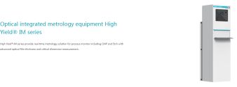
SiCarriers's metrology tools alone are enough to carry them. Materials analysis, optical metrology and electrical probes already makes a company - see KLA.

The fact that they also have at least RTP vacuum ovens is a plus. AMEC and ACM don't make those. And it isn't a huge leap from vacuum ovens to epitaxy and PVD, which they have too.

If it turns out in the end they're basically KLA + AMAT's PVD division, that's still a huge company.
 

tokenanalyst

Brigadier
Registered Member
SiCarriers's metrology tools alone are enough to carry them. Materials analysis, optical metrology and electrical probes already makes a company - see KLA.
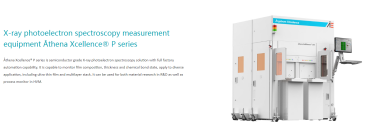
They have some differentiation in some tool, that is for sure, but in other areas they will have to compete with some already establish companies in China like Shenzhen Angstrom Excellence Technology Co. Ltd from their own hometown.

Please, Log in or Register to view URLs content!
 

tokenanalyst

Brigadier
Registered Member

The second phase of Tianjin Changlu New Materials Project started, expanding the application of electronic fluorinated liquid in chip manufacturing​


According to a news from Tianjin Economic Development Zone, Tianjin Changlu Chemical New Materials Co., Ltd. started construction of the second phase of the fluorine-containing organic new materials industrialization project on March 27. After completion, the project will become a fluorine chemical innovation base with international influence and a global high-end fluorine chemical industry chain base.
The Changlu New Materials Phase II project covers a total area of 120,800 square meters, with a total investment of 500 million yuan in the first phase. It will build two hydrofluoroether devices and supporting public works. After reaching full production, it will add 2,000 tons/year of production capacity and the annual output value will exceed 400 million yuan.

According to reports, at present, Tianjin Changlu Chemical New Materials Co., Ltd. has built a pilot industrialization base project for fluorine-containing organic new materials in Nangang Industrial Zone. Changlu New Materials will use the second phase project as a strategic fulcrum to accelerate the implementation of laboratory results into thousand-ton industrialization projects, expand the application of electronic fluorinated liquids in frontier scenarios such as chip manufacturing and data center immersion cooling , and jointly build a fluorine material innovation alliance with upstream and downstream companies, take the lead in compiling industry and group standards, and promote the in-depth development of domestic substitution. After the project is fully completed, it will become a benchmark for innovation in the high-end fluorine chemical industry in Beijing, Tianjin and Hebei.

Please, Log in or Register to view URLs content!
 

FairAndUnbiased

Brigadier
Registered Member
They have some differentiation in some tool, that is for sure, but in other areas they will have to compete with some already establish companies in China like Shenzhen Angstrom Excellence Technology Co. Ltd from their own hometown.

Please, Log in or Register to view URLs content!
They were established at about the same time tho, can you really say 1 is more established?
 

tokenanalyst

Brigadier
Registered Member

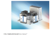
AMEC releases Primo Halona™, the first wafer edge etching tool, further improving the coverage of key etching processes​


During the SEMICON China 2025 exhibition, Shanghai Advanced Micro-Electronics Equipment Co., Ltd. (hereinafter referred to as "AMEC", stock code "688012.SH") announced the official release of its independently developed 12-inch wafer edge etching equipment Primo Halona™. The advent of this etching equipment by AMEC has achieved another breakthrough innovation in the field of plasma etching technology, marking the company's further progress towards the goal of comprehensive coverage of key processes, and also injecting strong momentum into the company's high-quality development.

This 12-inch edge etching equipment Primo Halona™ adopts the dual-reactor design with the characteristics of AMEC, which can flexibly configure up to three dual-reactor reaction chambers, and each reaction chamber can process two wafers at the same time, while ensuring low production costs, meeting the mass production needs of wafer edge etching, thereby achieving higher output density and improving production efficiency. In addition, the equipment chambers are equipped with Quadra-arm robotic arms, which are precise and flexible. The interior of the chamber is designed with corrosion-resistant materials to resist halogen gas corrosion, providing guarantees for the stability and durability of the equipment. In addition, Primo Halona™ is equipped with a unique self-alignment installation design, which can not only improve the centering accuracy and parallelism of the upper and lower plates, but also effectively reduce the downtime maintenance time caused by calibration installation, thereby helping customers optimize production capacity and lean production. In terms of equipment intelligence, Primo Halona™ provides an optional integrated measurement module. Customers can use this measurement template to achieve local real-time film thickness measurement, one-click compensation calibration of wafer transfer, and achieve better product maintainability, greatly improving the efficiency of later maintenance.​

1743079602529.png

Please, Log in or Register to view URLs content!
 

tokenanalyst

Brigadier
Registered Member
They were established at about the same time tho, can you really say 1 is more established?
Angstrom-E tools has been commercially available since the end of 2022 and in verification since 2020.
Looks like SiCarrier tools are only going to be commercially a available by mid 2025, if we give them 2 years of verification that would be 2023.
 
Top