Chinese semiconductor thread II

tokenanalyst

Brigadier
Registered Member

Meijie Optoelectronics received tens of millions of yuan in financing, focusing on the semiconductor mass testing equipment track​


Capital, Yida Capital recently completed a multi-million-yuan lead investment in Meijie Optoelectronics Technology (Shanghai) Co., Ltd. (hereinafter referred to as "Meijie Optoelectronics"). The funds from this round of financing will be used for Meijie Optoelectronics' investment in product research and development, team expansion and market expansion, further enhancing the company's product competitive advantage in the field of semiconductor mass testing equipment.
Meijie Optoelectronics was founded in 2015 and focuses on the research and development and manufacturing of semiconductor quality inspection equipment. The core team of Meijie Optoelectronics is composed of senior experts in the semiconductor industry. The founder Wen Renhua has rich industry experience and technical background, and has led the team to achieve significant breakthroughs in the fields of overlay equipment and defect detection equipment.
According to Yida Capital, Meijie Optoelectronics has successfully launched a variety of mass testing equipment, which are widely used in 8-inch and 12-inch semiconductor production lines, and has established close cooperative relationships with many leading domestic semiconductor manufacturers. The company is also developing advanced process mass testing equipment and is expected to deliver prototypes within the next two years to further promote the technological upgrade of domestic semiconductor mass testing equipment.
In January this year, the Meijie Optoelectronics Technology Headquarters Project with an investment of 850 million yuan was officially signed and landed in Wuxi. The company's headquarters will be located in Liyuan Development Zone and a semiconductor quantity detection equipment R&D and manufacturing base will be built.

Please, Log in or Register to view URLs content!
 

tokenanalyst

Brigadier
Registered Member
Ningbo Guanshi Semiconductor Photomask Manufacturing Project held a new product launch and line-up event.


On the morning of March 19, Ningbo Guanshi Semiconductor Photomask Manufacturing Project held a new product launch and line-up event. Wang Zhaobo, Director of Ningbo Qianwan New Area Management Committee and Deputy Secretary of the Party Working Committee, Wang Yidong, Director of Ningbo Economic and Information Bureau, Cai Shijie, Deputy Director of Ningbo Qianwan New Area Management Committee and Member of the Party Working Committee, and Li Yingzhong attended the event.

Ningbo Guanshi Semiconductor is a company specializing in the manufacture of semiconductor photomasks. Photomasks are graphic transfer tools or masters used in the photolithography process in microelectronics manufacturing, and their function is similar to the "film" of a camera. As one of the important raw materials in the upstream of the semiconductor industry chain, photomasks are carriers of intellectual property information such as graphic design and process technology. At present, my country's high-precision semiconductor photomask products still mainly rely on imports, and the localization rate is extremely low.

From the signing of the contract on May 16, 2023, the start of construction on October 1 of the same year, the completion and topping-out on January 27, 2024, to the current project being put into production, riding on the "east wind" of the "No. 1 Reform Project" to optimize and improve the business environment, in less than two years, Ningbo Guanshi Semiconductor has made rapid progress and achieved successive successes, completing fixed asset investment of more than 1 billion yuan and an effective investment intensity of more than 15 million yuan per mu, setting a new record for the Qianwan speed of the digital economy industry.

Currently, Ningbo Guanshi has achieved the delivery of 55nm photomask products and the completion of 40nm production lines. The company's products will be widely used in integrated circuit manufacturing fields such as artificial intelligence, high-performance computing, new energy vehicles, and consumer electronics. As a vivid epitome of driving innovation in Qianwan construction, the production of Ningbo Guanshi Semiconductor can be said to be an important part of the new district's semiconductor industry chain.

Please, Log in or Register to view URLs content!
 

tokenanalyst

Brigadier
Registered Member

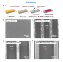
Using Higher Diffraction Orders to Improve the Accuracy and Robustness of Overlay Measurements.​

Abstract​

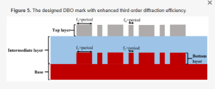
This paper introduces a method for improving the measurement performance of single wavelength overlay errors by incorporating higher diffraction orders. In this method, to enhance the accuracy and robustness of overlay error detection between layers, the measurement errors introduced by empirical formulas are corrected by incorporating higher diffraction orders, based on the differences in the light intensity difference curves for different diffraction orders. This method also expands the range of available wavelengths for selection. The introduction of specially designed overlay error measurement markers enhances the diffraction efficiency of higher diffraction orders to overcome the issue of their weak light intensity, making them difficult to utilize effectively. This paper first conducts a theoretical analysis using scalar diffraction theory, and then demonstrates the feasibility of the design through vector diffraction simulations and optical path simulations. The resulting two-layer marker structure is simple and compatible with existing measurement systems, showing tremendous potential for application at advanced process nodes.​

1742397681120.png

Please, Log in or Register to view URLs content!
 

tokenanalyst

Brigadier
Registered Member
Dual Ion Beam sputtering for EUV Mask Blanks. Looks like a commercial research by a domestic optical company.


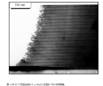
Multilayers with high normal incidence reflectivity in the extreme ultraviolet (EUV) spectral region are important focusing and imaging elements in EUV lithography (EUVL) [1], synchrotron applications [2] EUV microscopy [3], and X-ray astronomy [4]. The recent success of such multilayers is mainly due to the demand for EUV lithography, which is one of the leading candidates for the next generation of lithography [5–7]. EUVL is expected to cover several generations of devices with structure widths down to 30 nm. For this application, reflective coatings are required at wavelengths around 13.4 nm. EUVL applications require, in particular, high reflectivity, high uniformity, low surface and interface roughness, low stress, high temperature and photon flux stability, and low contamination effects. For multilayers of EUVL mask blanks, particle contamination levels must also be considered [8]. Few known material combinations can provide near normal high reflectivity. Promising results reported so far are based on multilayers of molybdenum (Mo) and silicon (Si) [9,10]. Deposition techniques such as electron beam evaporation [10,11], magnetron sputtering [9,12,13], pulsed laser deposition (PLD) [13] and ion beam sputtering deposition (IBD) [14] have been used to produce Mo/Si multilayers. Great success has recently been achieved using these techniques. EUV reflectivity of up to 70% has been reported in the case of interface engineered Mo/Si layer stacks [15]. However, one of the challenges and potential “roadblocks” facing EUVL technology is the need for extremely low defect density on the reflective EUV mask. IBD is considered to be the most favored deposition technique for EUVL masks due to its potential advantages compared to other deposition techniques such as conventional magnetron sputtering [16]. Therefore, we have initiated a program to investigate the properties of such ion beam sputtered reflective Mo/Si multilayers. Here, we will report on the preparation of Mo/Si multilayers by ion beam assisted deposition. We will present and discuss the results of characterization of the multilayers using microscopy, spectroscopy and diffraction techniques and compare them to data on Mo/Si mirrors from other deposition techniques.

1742401615875.png1742401708893.png1742401746100.png


5. Summary

Mo/Si multilayers for EUV lithography were prepared on Si wafer substrates using IBD. The multilayers were characterized by several experimental techniques including HR-TEM, TED, XRR, AFM, SIMS, PES, normal incidence reflectivity. The surfaces and interfaces of the multilayers appear quite smooth with relatively little roughness. Mixing and silicide formation at the Mo-Si interface and a multi-grained structure of the Mo layer are generally detected. Well-resolved multilayer diffraction spots, Kiessig fringes and other diffraction evidence indicate very good coherence of the wavefield, resulting in a multilayer period of 6.7 nm with good reproducibility. The normal incidence peak reflectivity in the EUV spectral range is 64-65% at 13.4 nm wavelength. The formation of EUV or soft X-ray standing wave fields is further confirmed using photoelectron spectroscopy. The results are discussed in comparison with other deposition techniques and new attempts at interface engineering are considered.
 

latenlazy

Brigadier
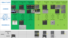
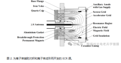
It can be basically confirmed that the domestic EUV light source does not follow the LPP carbon dioxide laser route of ASML, but the LPP multi-channel fiber laser sequence targeting route. The most critical high-pulse energy and high-repetition rate fiber laser has been produced and is completely domestically produced.


View attachment 148161

View attachment 148162
Please, Log in or Register to view URLs content!
If there is more than one team then we can’t conclude that.
 

tokenanalyst

Brigadier
Registered Member

Youde Diamond Heat Sink Wafers Achieve New Technological Breakthrough​


According to the official Weibo of Youde Diamond, Shenzhen Youde Diamond New Materials Technology Co., Ltd. (hereinafter referred to as "Youde Diamond") has recently made new technological breakthroughs in the field of diamond materials.

By optimizing the MPCVD process, Youde Diamond has successfully shortened the growth cycle of heat sink wafers and further increased the wafer size, providing a more efficient solution for the heat dissipation needs of high-power electronic devices.
1742407944495.png
According to reports, this technological breakthrough has achieved a dual upgrade in efficiency and size. By optimizing the production process and significantly increasing the deposition rate, it not only reduces the unit production cost, but also lays a technical foundation for large-scale mass production. While shortening the growth cycle, Youde Diamond has achieved a breakthrough in large-size wafers, meeting the needs of more high-power devices.​


Please, Log in or Register to view URLs content!
 

tokenanalyst

Brigadier
Registered Member

All solid-state single-frequency DUV source at 248 nm​


Abstract​

An all solid-state single-frequency 248 nm pulsed deep ultraviolet (DUV) source was realized based on multi-stage nonlinear frequency conversions of a 1064 nm fundamental driver. In detail, a 355 nm source, which is the third harmonic wave of 1064 nm laser, and an 827 nm source, which is the signal of an optical parametric oscillator (OPO) pumped by 532 nm laser, are combined for sum-frequency generation (SFG) to get the target wavelength of 248 nm. Finally, an average power of ∼120 mW was obtained at a 4 kHz repetition rate with a pulse width of 4.8 ns. The beam quality factor M2 was measured to be less than 1.5, and the linewidth was estimated to be ∼250 MHz. This method is compact, robust, and requires only one single and easily accessible 1064 nm fundamental driver. The presented 248 nm source could serve as an excellent seed for the KrF excimer laser amplifier to improve the beam quality and coherence.

Please, Log in or Register to view URLs content!
 

tokenanalyst

Brigadier
Registered Member

Theoretical investigation into effect of laser focal spot size on extreme ultraviolet radiation​

Abstract​

To understand the effect of laser focal spot size on the extreme ultraviolet conversion efficiency and the physical mechanism that produces the effect, we developed a two-dimensional transient expansion model of laser ablation of planar target to produce coronal plasma by means of theoretical analysis. It is found that under condition with light intensity of 7.45×10¹⁰ W/cm2, full width at half maxima of 5 ns, wavelength of 1064 nm, as the laser focal spot radius increases from 60 μm to 300 μm, the corresponding extreme ultraviolet conversion efficiency increases from 1% to 5.5%, while the corresponding extreme ultraviolet conversion efficiency stays at 5.5% after the focal spot radius is larger than 300 μm. This is due to the fact that the plasma in the coronal region generated by laser ablation of planar targets expands from the initial one-dimensional expansion to the subsequent two-dimensional expansion, which determines the saturation size of the plasma region emitting extreme ultraviolet light and ultimately determines the conversion efficiency of the extreme ultraviolet light. Our theoretical analysis on trend of conversion efficiency with focal spot radius can explain the physical phenomena observed in the laser ablation of a tin target experiment.​

Please, Log in or Register to view URLs content!
 
Top