Smartsens signing a deal with Nexchip for its 55nm platform's CIS Stack technique. Will be used to produce high end CIS chips as Smartsens enter more OEM's supply chain. So all revenue from fabbing to designing to packaging and testing all stay domestic.
You are using an out of date browser. It may not display this or other websites correctly.
You should upgrade or use an alternative browser.
You should upgrade or use an alternative browser.
Chinese semiconductor thread II
- Thread starter vincent
- Start date
If you admit that Ascend yield has double in a year, then the obvious conclusion is that yield for Kirin line of chips has also increased significantly. Based on 40% yield (which I think doesn't fully account for binning), you get a > 80% yield on Phone SoC sized chips. Assuming obviously if you get some defect on the more complicated SoC, you bin aggressively and put it in lower line of chips. And they have even smaller SoC like Kirin 8000 line (which is now on even Enjoy series). So yeah, the production of Kirin chips likely to be greater than 50 million this year.
Let's say Huawei gets 60 million chips this year and they get on average 480 chips per wafer as my screenshot shows, then that is 125000 wafers, so greater than 10k wpm from this. If they get 80 million chips this year, then we are look at 14k wpm from this.
Adding in 3 to 4k wpm from Ascend and Kunpeng chips, there is still several k wpm from other domestic chipmakers like Phylum, Moore Thread, Biren and others.
I would not be surprised if they get close to 25k wpm of 7nm (or better) capacity by second half of this year and then 40-50k wpm by 2026.
CR Micro's MOS and SiC products are used in AI server power supplies and are expected to achieve high growth
China Resources Microelectronics issued an investor relations activity record sheet announcement. The announcement pointed out that the company's current medium and low voltage MOS, high voltage MOS, and SiC products can be used in AI server power supplies and are already in the mass production stage. SiC JBS and SiC MOS have completed product serialization and achieved mass production. The products cover 650V/1200V/1700V series, and the performance has reached the same level as the international leading level. In addition, silicon carbide module products are also in the mass production stage. China Resources Microelectronics' products are fully promoted and increased in volume in the fields of new energy vehicles, charging piles, photovoltaic inverters, energy storage inverters, server power supplies, etc., and are expected to achieve high growth this year.
China Resources Microelectronics issued an investor relations activity record sheet announcement. The announcement pointed out that the company's current medium and low voltage MOS, high voltage MOS, and SiC products can be used in AI server power supplies and are already in the mass production stage. SiC JBS and SiC MOS have completed product serialization and achieved mass production. The products cover 650V/1200V/1700V series, and the performance has reached the same level as the international leading level. In addition, silicon carbide module products are also in the mass production stage. China Resources Microelectronics' products are fully promoted and increased in volume in the fields of new energy vehicles, charging piles, photovoltaic inverters, energy storage inverters, server power supplies, etc., and are expected to achieve high growth this year.
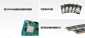
Aikosa Technology completes a new round of financing and moves its headquarters to Chengdu to accelerate the innovation of aerospace storage technology
Xi'an Aikesa Technology Co., Ltd. (hereinafter referred to as "Aikesa Technology"), a leading company in the commercial aerospace storage segment in China, recently announced the completion of a new round of financing led by Chengdu Science and Technology Venture Capital. The company simultaneously completed the change of industrial and commercial registration, officially changed its name to Aikesa Technology (Chengdu) Co., Ltd., and moved its headquarters to Chenghua District, Chengdu, marking the company's entry into a new stage of large-scale development. This round of financing will focus on the establishment of cutting-edge technology R&D centers and the increase of aerospace-grade SSD mass production capacity, accelerating the construction of a moat in the field of aerospace storage.
Having core products and hard-core strength is the key to Chengdu Science and Technology Investment Group's investment in Aikosa Technology. The investment in Aikosa and its attraction to Chengdu has injected new momentum into Chengdu's creation of a modern aerospace industry cluster with distinctive characteristics, concentrated factors, intelligent high-end, open and independent. In the future, the Science and Technology Investment Group will continue to focus on strong support for enterprises, serve the development of the private economy around "expanding the market, reducing costs, providing scenarios, and building platforms", relying on the group's scientific and technological resources and industrial advantages, and further promote the function of state-owned enterprises to "optimize and strengthen enterprises", and provide comprehensive post-investment empowerment for Aikosa.
Aerospace grade SSDs.

Can you estimate the core die size of 910c using the Smic process and 53B transistors (from an article in tomshardware)?
If you admit that Ascend yield has double in a year, then the obvious conclusion is that yield for Kirin line of chips has also increased significantly. Based on 40% yield (which I think doesn't fully account for binning), you get a > 80% yield on Phone SoC sized chips. Assuming obviously if you get some defect on the more complicated SoC, you bin aggressively and put it in lower line of chips. And they have even smaller SoC like Kirin 8000 line (which is now on even Enjoy series). So yeah, the production of Kirin chips likely to be greater than 50 million this year.
Let's say Huawei gets 60 million chips this year and they get on average 480 chips per wafer as my screenshot shows, then that is 125000 wafers, so greater than 10k wpm from this. If they get 80 million chips this year, then we are look at 14k wpm from this.
Adding in 3 to 4k wpm from Ascend and Kunpeng chips, there is still several k wpm from other domestic chipmakers like Phylum, Moore Thread, Biren and others.
I would not be surprised if they get close to 25k wpm of 7nm (or better) capacity by second half of this year and then 40-50k wpm by 2026.
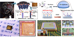
"Core" achievements | The latest IEDM of the college research team: wide-angle and wide-spectrum compound eye chip
A team led by Professor Xu Yang and Professor Yu Bin from the School of Integrated Circuits at Zhejiang University and Researcher Wen Liaoyong from Westlake University proposed a wide-angle and wide-spectrum compound eye CMOS chip. The work was published in IEDM under the title “First Demonstration of 2.5D Out-of-Plane-Based Hybrid Stacked Super-Bionic Compound Eye CMOS Chip with Broadband (300-1600 nm) and Wide-Angle (170°) Photodetection”.
Xie Yunfei and Wang Xiaochen, PhD students at the School of Integrated Circuits, Zhejiang University, and He Jing, PhD student at Westlake University, are the co-first authors. This work was supported by the National Key R&D Program, the National Natural Science Foundation of China, the Tape-out Program of the School of Integrated Circuits, Zhejiang University, and the Institute of Optoelectronics, Westlake University.

Multiply die size by 2.Can you estimate the core die size of 910c using the Smic process and 53B transistors (from an article in tomshardware)?
Last edited:
Probably because of communication issues between two dies and a less advanced node. 910c and Blackwell will be two difficult GPUs to work with as they are the first GPUs with chiplet architect. AMD faced similar issues with Zen 1 and Zen 2.
