Chinese semiconductor thread II

tokenanalyst

Brigadier
Registered Member

A number of semiconductor projects were signed in Quzhou involving gallium oxide, aluminum nitride single crystal substrates, etc.​

The projects signed on site involved multiple semiconductor-related projects, including Zhejiang Xin Gu Semiconductor Industrial Park, semiconductor core components project, aluminum nitride single crystal substrate project, and 6-inch compound substrate project.
Zhejiang Core Valley Semiconductor Industrial Park
The project plans to invest a total of 1.77 billion yuan, covering an area of 221 mu, to build the Zhejiang Core Valley Semiconductor Industrial Park. After reaching full production, it is expected to achieve an annual operating income of 1.8 billion yuan and an annual tax revenue of 90 million yuan.
Semiconductor core components project
The project plans to invest a total of 1 billion yuan, lease a plant of 54,000 square meters, and build an annual production capacity of 200,000 stacked piezoelectric ceramic actuators, 100,000 high-power piezoelectric ceramic transducers, 3,100 silicon parts silicon rings/silicon shower heads, and 105,000 sets of semiconductor core parts. After reaching full production, it is expected to achieve an annual operating income of 660 million yuan and an annual tax of 65 million yuan.
Aluminum nitride single crystal substrate project
The project plans to invest a total of 1 billion yuan, covering an area of 150 mu, and build a production line with an annual output of 50,000 pieces of 2-6 inch AlN single crystal substrates. After reaching full production, it is expected to achieve an annual operating income of 1 billion yuan and an annual tax revenue of 150 million yuan.
6-inch compound (gallium arsenide, indium phosphide, gallium oxide) substrate project
The project plans to invest a total of 1 billion yuan, covering an area of 30 mu, and building a plant of about 20,000 square meters, mainly to build a 6-inch compound substrate production line. After reaching full production, it is expected to achieve an annual operating income of 1 billion yuan and an annual tax revenue of 50 million yuan.

Please, Log in or Register to view URLs content!
 

tokenanalyst

Brigadier
Registered Member

Qingdao, Shandong, a 1 billion yuan semiconductor equipment project landed

According to the "Qingdao West Coast Release" public account, on February 5, the semiconductor equipment R&D and production headquarters project with a total investment of 1 billion yuan by Haichuang Intelligent Equipment (Yantai) Co., Ltd. settled in Qingdao West Coast New Area.
According to information, Haichuang Intelligent Equipment (Yantai) Co., Ltd. was established in 2017 with a registered capital of 80 million yuan. It is committed to the research and development, manufacturing and sales of high-end semiconductor equipment and has more than 60 related patents.
According to reports, as the second semiconductor high-end equipment project to be implemented in Qingdao West Coast New Area since 2025, the project will select a site in the new area to build a semiconductor equipment R&D and production headquarters, to develop and manufacture wafer-level permanent bonding, temporary bonding, and debonding equipment and other products. It plans to combine domestic industry needs and its own technological advantages to develop into a well-known domestic semiconductor equipment company.

Please, Log in or Register to view URLs content!
 

Overbom

Brigadier
Registered Member
Apple shipped around 75M phones in Q4 2024, for comparison. 13M a quarter is really not that much.
13m a quarter with the entire US Empire going full ballistic against it. Now that the king has returned, I very much doubt this will stay like this. I expect a huge increase. Huawei is coming for everyone, is coming for your phone, for your OS, for your network, for self-driving, for EV tech etc, it's coming for everything

Bonus point: Huawei's phones are almost entirely domestically made. Vast majority of value added parts, manufacturing and R&D is all domestic
 

tphuang

General
Staff member
Super Moderator
VIP Professional
Registered Member

tokenanalyst

Brigadier
Registered Member

China's photon millimeter wave radar has made a major breakthrough, and L4 autonomous driving is coming!​


According to official news from Nankai University, recently, the team led by Academician Zhu Ninghua of the Institute of Intelligent Photonics of Nankai University, in cooperation with the City University of Hong Kong , successfully developed the world's first integrated thin-film lithium niobate photonic millimeter-wave radar based on a 4-inch thin-film lithium niobate platform , achieving breakthrough progress in centimeter-level distance and speed detection resolution and inverse synthetic aperture radar (ISAR) two-dimensional imaging . This achievement not only marks China's technological leadership in the field of microwave photonics, but also lays a key foundation for intelligent sensing applications in the 6G era.

1738947595074.png

This time, the Nankai University and City University of Hong Kong team used material innovation, using thin-film lithium niobate materials with high linear electro-optic coefficients, wide wavelength transparent windows, and large refractive index differences , combined with a 4-inch wafer platform compatible with CMOS processes, to achieve high-performance electro-optic modulation. Compared with traditional silicon-based materials, the electro-optic conversion efficiency of thin-film lithium niobate has increased by an order of magnitude, and supports higher frequency (up to 300 GHz) and larger bandwidth (more than 10 times that of traditional radar) signal processing capabilities. As shown below:

At the same time, a breakthrough was also achieved in technology. Through the optimization of UV step-by-step lithography and dry etching processes , the team integrated the radar's frequency multiplication module, echo de-skewing module and other functions into a chip of only 15 mm × 1.5 mm × 0.5 mm , which is only one thousandth the size of a traditional discrete radar system . This design not only simplifies the complexity of the system, but also breaks through the performance limitations of high-speed analog-to-digital converters (ADC/DAC), realizes the integration of on-chip millimeter-wave signal generation and echo processing, and significantly improves signal processing efficiency and anti-interference capabilities.

Due to breakthroughs in core materials and core technologies, the application of microwave photon radar is also expected to develop towards higher frequency, larger bandwidth and smaller size , triggering revolutionary applications in many fields such as automotive radar, airborne radar and smart home .

Please, Log in or Register to view URLs content!
 

tokenanalyst

Brigadier
Registered Member

Zhanxin Electronic Technology Co., Ltd. recently announced the successful completion of the first round of funding in its Series C financing, raising nearly RMB 1 billion.​


This round of financing was led by China Development Bank Manufacturing Transformation and Upgrading Fund, followed by CICC Capital, Goldstone Investment and Xinxin Capital.

According to public information, since its establishment in 2017, Zhanxin Electronics has focused on the research and development of silicon carbide power devices, drive and control chip products, and is located in the middle stream of the silicon carbide industry chain.

To date, Zhanxin Electronics has completed seven rounds of financing with a total financing amount exceeding 2 billion yuan.

Investors include many well-known industrial capital and financial investment institutions, such as Xiaomi Industrial Investment, SAIC, Star Capital, GAC Capital, BAIC Industrial Investment, Linxin Investment, SDIC Innovation, Lightspeed Photosynthesis, Guofang Innovation and New Area Fund.

previously, it also received strategic financing from Xiaopeng Motors' exclusive investment, as well as a Pre-B round of financing jointly led by SAIC Group's Strategic Direct Investment Fund and Shangqi Capital.

Please, Log in or Register to view URLs content!
 

tokenanalyst

Brigadier
Registered Member
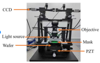
Lithography is about precision.

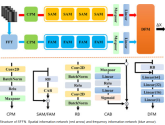
Small-area marks realize nanoscale lithography alignment by a spatial and frequency domain fusion neural network​

Abstract​


For traditional moiré-based lithography alignment technology, which is widely used in proximity lithography systems, complex alignment marks with larger areas are employed to achieve high-precision misalignment detection. However, every inch of space on the wafer is extremely precious in practice, leaving minimal space for alignment marks. Therefore, employing small-area alignment marks in lithography systems will be a very challenging task with considerable potential in the future. The primary challenge is that existing frequency-based analytical algorithms struggle to achieve misalignment values with high-precision from moiré fringe images generated by small-area marks. To address this challenge, a spatial and frequency information fusion neural network (SFFN) is proposed for processing the moiré fringe images. With SFFN, the area of the alignment mark can be reduced by 2/3, and the average error of SFFN is less than 1 nm on the test dataset.

1738957721555.png1738957770331.png
1738957796983.png

Please, Log in or Register to view URLs content!
 

tokenanalyst

Brigadier
Registered Member

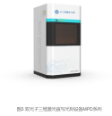
Yuzhiquan Femtosecond Laser Direct Writing Lithography System: Building the Engineering Power of the Microscopic World.​


In order to promote the development of domestic direct writing lithography technology, the country has introduced a number of positive policies to vigorously support related industries to carry out theoretical and technological innovation, and support multiple laboratories to carry out related research. Hangzhou Yuzhiquan Precision Instruments came into being. The company's research results and founding team mainly come from Zhejiang University. In recent years, the research team has made a lot of original design work in the field of two-photon lithography , specifically covering the development of new high-performance photoresists , the improvement of femtosecond laser direct writing lithography efficiency , and the development of advanced lithography systems . The many academic papers and patents published have been highly praised by many well-known experts and scholars at home and abroad . With the unremitting efforts of the team, the optimal accuracy of the laser direct writing system was finally improved to the sub- 50 nm scale ; and in the ten-channel laser direct writing system developed by it, the writing flux even reached an astonishing level of 100 M/S . After continuous iteration of the company, the new generation of commercial two-photon three-dimensional laser direct writing lithography equipment MPD series has been officially sold in 2022.

1738960410644.png

1738960357122.png1738960381012.png

Please, Log in or Register to view URLs content!
 
Top