Chinese semiconductor thread II

FairAndUnbiased

Brigadier
Registered Member
I'd just like to give a brief introduction to this topic.

For those who aren't as familiar, this is a EUV photoresist. You can easily tell just by looking at it because this is an organometallic compound containing In, which has a high EUV absorption cross section.

Please, Log in or Register to view URLs content!

images

the purpose of the organic component is to change solubility. when the metallic component absorbs energy from the EUV illumination, it transfers that through bond breaking/reforming with the organic component, which changes its solubility.

There are challenges for a EUV photoresist which includes low outgassing in vacuum environments (does not contaminate lithography chamber), high resolution (only what is illuminated has photochemical reaction), high contrast (very different developer solution solubility for illuminated/nonilluminated regions) and nanoscale dimensional stability (does not change shape when placed in developer solution).
 

latenlazy

Brigadier
I'd just like to give a brief introduction to this topic.

For those who aren't as familiar, this is a EUV photoresist. You can easily tell just by looking at it because this is an organometallic compound containing In, which has a high EUV absorption cross section.

Please, Log in or Register to view URLs content!

images

the purpose of the organic component is to change solubility. when the metallic component absorbs energy from the EUV illumination, it transfers that through bond breaking/reforming with the organic component, which changes its solubility.

There are challenges for a EUV photoresist which includes low outgassing in vacuum environments (does not contaminate lithography chamber), high resolution (only what is illuminated has photochemical reaction), high contrast (very different developer solution solubility for illuminated/nonilluminated regions) and nanoscale dimensional stability (does not change shape when placed in developer solution).
Photon transfer stuff always make me go wheee *it’s such a cool part of chemistry*.
 

tokenanalyst

Brigadier
Registered Member

Shuoke Crystal launches the world's first 12-inch high-purity semi-insulating silicon carbide substrate​


Shanxi Shuoke Crystal Co., Ltd., an enterprise in Shanxi Transformation and Comprehensive Reform Demonstration Zone, has recently successfully developed a 12-inch (300mm) high-purity semi-insulating silicon carbide single crystal substrate, which is the first in the world. At the same time, it also successfully developed a 12-inch (300mm) N-type silicon carbide single crystal substrate.

According to reports, Shanxi Shuoke Crystal Co., Ltd. is a domestic enterprise engaged in the production and research and development of silicon carbide, a third-generation semiconductor material. In recent years, through independent innovation and independent research and development, Shuoke Crystal has fully mastered the manufacturing of silicon carbide growth equipment and the preparation process of high-purity silicon carbide powder. It was the first in China to complete the key process technology research of high-purity semi-insulating silicon carbide single crystal substrates, and has successively conquered the large-size diameter expansion process and the growth process of low-defect N-type substrates. It has a complete set of production lines for silicon carbide powder preparation, single crystal growth, and wafer processing. The successful development of the 12-inch silicon carbide substrate can further expand the area on a single wafer that can be used for chip manufacturing and greatly increase the output of qualified chips. Under the same production conditions, it can significantly increase production, reduce unit costs, and further improve economic benefits, providing possibilities for larger-scale applications of silicon carbide materials.

It is reported that the core team of Shuoke Crystal has been committed to the research and development of silicon carbide materials since 2009, covering silicon carbide growth equipment manufacturing, powder synthesis, crystal growth and substrate processing, and has successively made breakthroughs in core technical difficulties such as high-purity silicon carbide powder synthesis technology, low-defect large-diameter silicon carbide single crystal growth process technology and ultra-flat silicon carbide substrate processing technology.

Please, Log in or Register to view URLs content!
 

tokenanalyst

Brigadier
Registered Member

Four domestic 12-inch wafer production lines put into production!​


For example, the four 12-inch wafer production lines of Runpeng Semiconductor, Tiancheng Advanced, CanSemi, and Huahong Wuxi have all recently announced the start of production; Yandong Microelectronics announced that it plans to issue an additional 4.02 billion yuan to the actual controller to invest in the construction of a 12-inch integrated circuit production line; two wafer production lines including SMIC and Guangzhou Zengxin Technology have also made new progress, focusing on the production of power devices and logic ICs.
The Shenzhen Runpeng Semiconductor 12-inch wafer production line project held a line-opening ceremony on December 31 last year. The total investment in the first phase of the project is RMB 22 billion, focusing on processes above 40nm, and is mainly used in automotive electronics, new energy, consumer electronics and other fields.

Please, Log in or Register to view URLs content!
 

tokenanalyst

Brigadier
Registered Member

Zhixian Future won the title of "Shenzhen Specialized, Refined and New Small and Medium Enterprises"​


Zhixian Future has long been focusing on the research and exploration of intelligent technology in semiconductor engineering to promote the in-depth development of technology.

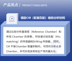
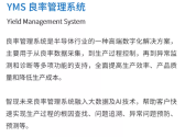
By integrating big language model technology into engineering intelligence systems, we provide high-end manufacturing customers with a full range of intelligent management solutions, helping them to achieve efficient and reliable improvements in yield, production efficiency and product output. The company's multiple "big model + engineering intelligence" fusion products have been successfully implemented and accepted in 12-inch wafer fabs, which not only significantly improved customers' production efficiency and yield, but also attracted the attention and cooperation of many top customers, further expanding market opportunities. At present, the AI-enabled engineering intelligence product system has fully covered a complete closed loop including equipment monitoring, intelligent yield analysis, defect management, intelligent prediction and intelligent decision-making.
1736174682485.png1736174787061.png
1736174851373.png1736174892025.png


In terms of business layout, Zhixian Future has been expanding horizontally, transferring its advantages in the semiconductor industry to more sub-industries such as new energy, high-end chemicals, and new power systems. Taking the lithium battery industry as an example, Zhixian Future successfully won the "Lighthouse Factory" construction project of a domestic lithium battery giant with its excellent and reliable engineering intelligent solutions, helping it to achieve real-time monitoring and precise control of the production process, improve production efficiency, reduce production costs, and further optimize product quality.

So far, Zhixian Future has provided engineering intelligence products and services to more than 160 benchmark companies including Huahong Grace, CRRC Times, Jiejie Micro, Xinsheng, Eswin, Huaxing Optoelectronics, BOE, Tianma, SMIC Shaoxing, and Samsung, significantly improving customers' production efficiency and value. In the future, we will deepen the horizontal expansion of our business and enable more high-end manufacturing customers to achieve intelligent transformation.

Please, Log in or Register to view URLs content!
 

tokenanalyst

Brigadier
Registered Member

Another semiconductor key material project landed in Xi'an Economic Development Zone​

Xi'an Economic Development Zone and Tangshan Holding Development Group held a project signing ceremony. Tangshan Holding Development Group plans to invest 500 million yuan to build production lines, R&D centers and supporting facilities including semiconductor photosensitive agents (PAC & PAG), phenolic resins and additives in the Economic Development Zone. After the project is completed, it will further improve and extend the semiconductor industry chain, while realizing the domestic substitution of multiple semiconductor materials, effectively improving the security and independent control level of the electronic information industry chain, and injecting new vitality into regional economic development.
It is reported that as an innovation cluster of new materials industry in Shaanxi Province, Xi'an Economic and Technological Development Zone has been constantly exploring and innovating in the research and development and application of new semiconductor materials, forming a semiconductor industry cluster supported by leading enterprises such as Huatian Technology, Huayi Microelectronics, and Longteng Semiconductor, represented by packaging and testing, high-end integrated circuits, and power semiconductor device research and development. The zone is making every effort to build a semiconductor materials industrial park.

Please, Log in or Register to view URLs content!
 
Top