Chinese semiconductor thread II

tokenanalyst

Brigadier
Registered Member

Shanghai: Launch of 11 key laboratories including wide bandgap and ultra-wide bandgap semiconductor materials​


On December 31, 2024, the Shanghai Science and Technology Commission issued a notice. According to the relevant provisions of the "Shanghai 2024 Science and Technology Innovation Action Plan Key Laboratories (First Batch) Application Guidelines" and the "Shanghai Key Laboratory Construction and Operation Management Measures" (Shanghai Science and Technology Regulation [2022] No. 6), it will coordinate with the recommending departments to review and demonstrate, and start the preparation and establishment of 11 key laboratories including the "Shanghai Key Laboratory of Wide Bandgap and Ultra-Wide Bandgap Semiconductor Materials".
Among them, the supporting institutions of Shanghai Key Laboratory of Wide Bandgap and Ultra-Wide Bandgap Semiconductor Materials (under preparation) are: Shanghai Tianyue Semiconductor Materials Co., Ltd. and Shanghai Institute of Optics and Precision Mechanics, Chinese Academy of Sciences.

Please, Log in or Register to view URLs content!
 

tokenanalyst

Brigadier
Registered Member

Beijing Integrated Circuit Equipment Investment and Merger Phase II Fund was established with a capital contribution of RMB 2.5 billion​


According to the Qichacha APP, Beijing Integrated Circuit Equipment Industry Investment and Merger Phase II Fund (Limited Partnership) was established recently with a capital contribution of 2.5 billion yuan. Its business scope includes: engaging in equity investment, investment management, asset management and other activities with private equity funds. Qichacha's equity penetration shows that the company is jointly funded by North Huachuang Innovation Investment (Beijing) Co., Ltd., a wholly-owned subsidiary of North Huachuang (002371), Beijing State-owned Capital Operation Management Co., Ltd., and Beijing Integrated Circuit Industry Investment Fund (Limited Partnership)

Please, Log in or Register to view URLs content!
 

Wahid145

Junior Member
Registered Member

This is very interesting for Huahong. Hopefully this means they are making a bigger push in advanced nodes.
Having experience in Intel does not sound very appealing considering the absolute mess Intel is in right now. But lets hope he was one of the better ones in Intel.
He also worked on Rong Semi (a company established in 2021).
Please, Log in or Register to view URLs content!

I wonder how that company is faring after 4 years. Apparently they are mass producing upto 55nm as of now.
 
Last edited:

tokenanalyst

Brigadier
Registered Member

Zhaoxun Hengda: The first industrial-grade security MPU is launched to help upgrade the industrial manufacturing industry.​


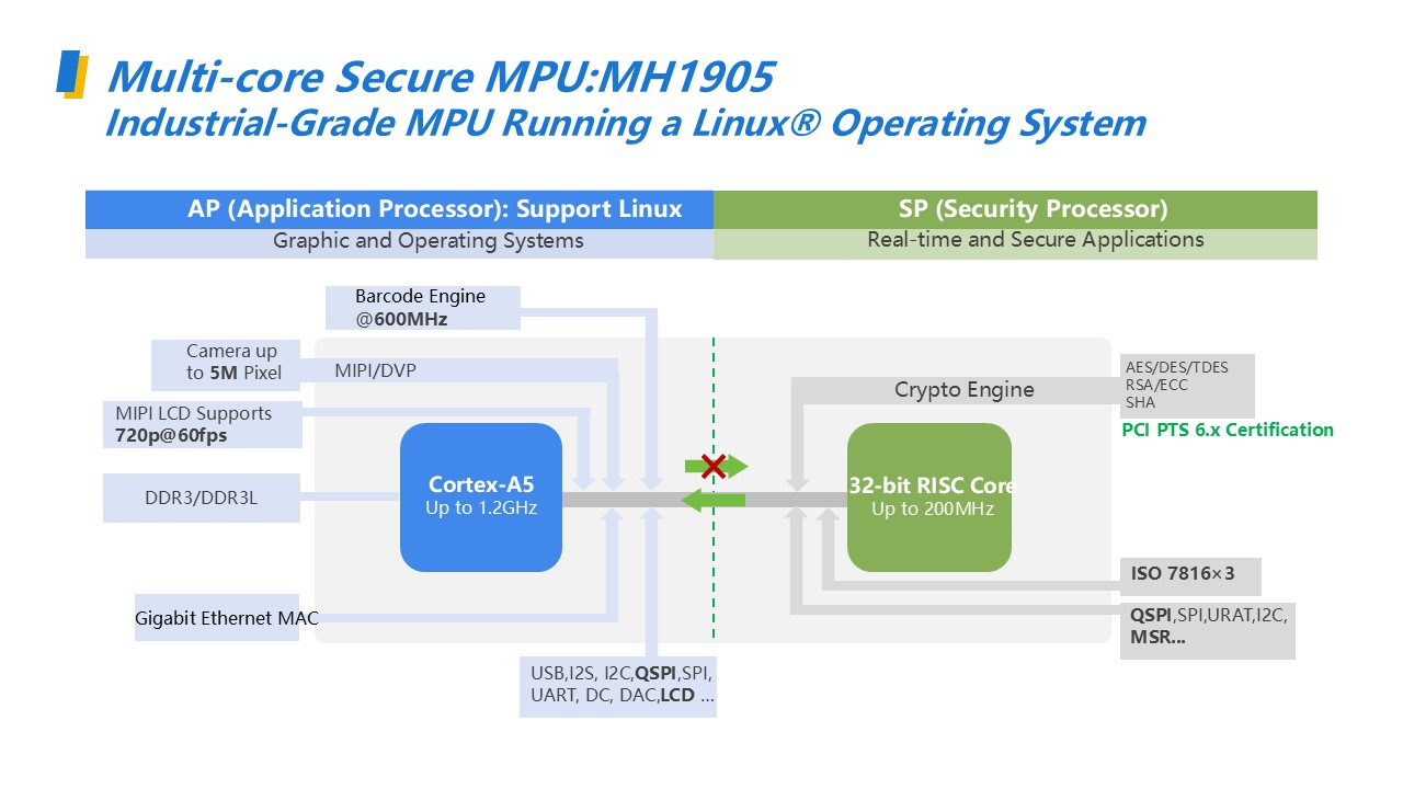
Zhaoxun Hengda announced the launch of its latest research and development results - MH1905. The product is built on a heterogeneous asymmetric architecture and integrates a high-performance application processor (AP) and a security processor (SP), bringing disruptive solutions to consumer electronics, industrial control, the Internet of Things and other fields.

1226216889803.1316.png

Specifically, the AP system of MH1905 uses the ARM Cortex-A5 core, with a maximum operating frequency of up to 1.2GHz, which can easily handle complex operating system tasks. At the same time, it supports 720p resolution video output and up to 5 million pixel camera access, providing strong support for applications such as image processing and video surveillance. In addition, the AP is also compatible with multiple memory types and integrates a Gigabit Ethernet MAC to meet the needs of high-speed data transmission.

1711235810739.1914.png
1735908652163.png

Figure 2

In terms of security, the SP processor of MH1905 also performs well. It uses a 32-bit RISC core with a maximum operating frequency of 200MHz, focusing on the processing of real-time and security applications. SP has a built-in powerful encryption engine, supports multiple encryption algorithms such as AES, DES, TDES, RSA, ECC, SHA, and provides hardware encryption acceleration. In addition, SP also has anti-tampering pins, sensitive data such as key storage areas powered by button batteries, and data retention time of more than five years; it also has anti-tampering functions, providing all-round protection for data security. [See Figure 2]

It is worth mentioning that the two subsystems of the MH1905 processor exchange data through an efficient cross switch, ensuring the collaborative work between the AP and the SP. At the same time, the processor also shares a variety of peripheral interfaces, such as USB, I2C, SPI, etc., and provides practical functions such as general input and output interface (GPIO) and barcode engine, further enhancing its application flexibility. In addition, MH1905 adopts advanced FCCSP packaging technology, with a size of 13 x 13mm, 361 solder balls, and a pitch of 0.65mm, which is very suitable for embedded applications.

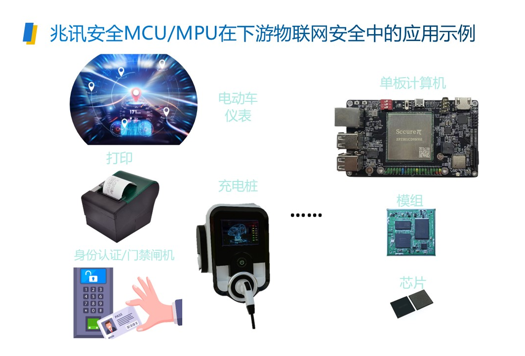
MH1905's unique dual-subsystem architecture not only improves the performance and security of the processor, but also provides a more comprehensive and efficient solution for various application scenarios. In order to facilitate customers and enthusiasts to quickly get started with development, Zhaoxun Hengda has launched the SecurePi series modules based on MH1905 with its partners, including SP2301, SP2302, etc., which are suitable for application scenarios of various electronic devices.

Please, Log in or Register to view URLs content!
 

tokenanalyst

Brigadier
Registered Member

SGSSEMI high-end semiconductor equipment project signed and landed in Huishan.​

he Shengjisheng high-end semiconductor equipment project was signed and landed in Huishan. In the future, it will be located in the Huishan Advanced Manufacturing Industrial Park which is about to be put into use, adding strong momentum to the leap forward of Huishan's semiconductor industry.

Shengjisheng Intelligent Equipment (Jiangsu) Co., Ltd. was established in December 2022. It is an enterprise focusing on the research and development, manufacturing and sales of high-end equipment in the field of advanced semiconductor packaging and packaging testing. Its main products are nano-scale hybrid bonding equipment, high-speed and high-precision placement machines, test sorting machines, etc., and its technical level is internationally leading. The company has gathered outstanding talents from top international semiconductor companies, with more than 40 R&D personnel, more than 50% of whom have a master's degree or above. It currently has two subsidiaries, SGSSEMI (SINGAPORE) PTE. LTD. and Suzhou Shengmao Micro Technology Co., Ltd. The company's products have now entered domestic benchmark customers such as SMIC.

The project has an initial investment of 500 million yuan, and will build an internationally leading semiconductor equipment R&D, production and sales center around its core equipment, striving to achieve a sales order of 100 units or more within three years; the second phase will add production lines to further expand production capacity.​

Please, Log in or Register to view URLs content!
 

tokenanalyst

Brigadier
Registered Member

HGTECH: 400G silicon photonic modules shipped in batches, 800G LPO products to be put into production soon​

Recently, HGTECH released a record of investor relations activities, stating that in terms of the company's connection business, 400G silicon photonic modules have been shipped in batches to leading domestic Internet manufacturers, and will continue to increase in volume in the future. HGTECH's optical module production base construction project in Wuhan is about to open a new chapter in accelerating optical module production. The company's overseas production base in Thailand is mainly based on 800G and 1.6T demand, with a planned monthly production capacity of 100,000 units, and plans to quickly increase to 200,000 units based on customer demand.
1735909264548.png
800G LPO products are about to be put into mass production and overseas production capacity is increasing rapidly

In terms of overseas markets for optical connection business, the company said that it has tested 400G, 800G and 1.6T products with many leading customers. 800G LPO products have received clear demand and are currently being tested and introduced as soon as possible. 1.6T products are being tested at an accelerated pace, and the overall progress is in the first echelon of the industry. The company's overseas factories for optical connection business have achieved production conditions and are preparing for the volume increase of 800G LPO products in the first quarter of next year.

In September 2024, the company launched a new 800G AEC module, which is suitable for connections between servers, switches and routers. It can provide stable and high-speed data transmission while reducing signal attenuation and interference, and supports 400G/800G data transmission rates, which is crucial for intelligent computing centers and supercomputing centers that handle large-scale data and complex computing tasks. The company expects that market demand will be released next year, and the company will actively promote the adaptation of this product among target customers.

At the same time, the company has also accelerated the construction of overseas factories, which have now reached production status. Overseas demand is mainly for 800G and 1.6T. The planned monthly production capacity is 100,000 units, and it is planned to quickly increase to 200,000 units based on customer demand.

Please, Log in or Register to view URLs content!
 

tokenanalyst

Brigadier
Registered Member

Laipu Technology's integrated circuit equipment R&D and manufacturing base project will be put into production this year.​

The Laipu Technology National Headquarters and Integrated Circuit Equipment R&D and Manufacturing Base Project will be put into production this year. At the site of the Laipu Technology National Headquarters and Integrated Circuit Equipment R&D and Manufacturing Base Project (hereinafter referred to as the "Laipu Technology Project"), it can be seen that the interior and exterior decoration of the project has been basically completed. Compared with three months ago, the project is covered with a layer of silver-white shell, and the previously empty windows have been decorated with glass.
The project has now officially entered the final stage and will be put into production this year. The Laipu Technology project covers an area of 39 acres and a construction area of 65,000 square meters. The main construction content includes the company's national headquarters, technology center, manufacturing center, service center, and core component R&D and industrialization base. It will also simultaneously build the Chengdu Semiconductor Materials Advanced Laser Processing Technology Joint Laboratory and Training Base of the Semiconductor Institute of the Chinese Academy of Sciences, and the Sichuan Province All-Solid State Advanced Laser Engineering Technology Research Center and other projects.
After the project is completed, it will strongly promote the advancement of laser equipment and technology in my country's semiconductor field, and play a positive role in front-end process innovation in integrated circuit manufacturing, application and system integration of advanced laser technology, independent control of core components, and training of professional talents.

SIC and IGBT annealing
1735911380468.png
Laser junction activation equipment and Marking equipment
1735910007592.png

Laser induced Epitaxial growth equipment
1735910041077.png

Please, Log in or Register to view URLs content!

 
Top