Chinese semiconductor thread II

european_guy

Junior Member
Registered Member

Please, Log in or Register to view URLs content!


Please, Log in or Register to view URLs content!

According to a recent Citigroup analysis:

CXMT, China's domestic memory chipmaker, is demonstrating significant progress in its DDR5 production yields. The company's DDR5 yield rates had reached approximately 80%, marking a substantial improvement from its initial 50% yields when production began. This progress builds on CXMT's experience with DDR4 manufacturing, where the company has achieved yields of around 90%. The company currently operates two fab facilities in Hefei, with Fab 1 dedicated to DDR4 production on 19 nm process technology and a 100,000 wafer per month capacity. Fab 2 focuses on DDR5 production using 17 nm technology, with a current capacity of 50,000 wafers per month. CXMT's DDR5 yields could improve further to approximately 90% by the end of 2025.

This X thread seems better reporting Citigroup original study:

Please, Log in or Register to view URLs content!

GfzEn-eacAAfpPv.jpg

Currently 150K wpm, to add additional 50K wpm within next year:

GfzEpGkaUAAlC1u.jpg


Well, that's quite a lot of juicy stuff! In particular, it is the first time I read (from some credible source) that HBM 2 is sampling to customers now. This is big if confirmed.

HBM 2 low volume production in Q2 2025...I have an idea who will be the first customer :)
 

european_guy

Junior Member
Registered Member
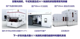
He talked about working station development for lithography machine. He said that his team developed working stations for 90/65/28 nm DUV machines. Also developed prototype machines for EUV

Please, Log in or Register to view URLs content!

For the record, the guy who is talking is from Huazhong University of Science and Technology (HUST) and it seems thay developed an active anti-vibration platform for lithographic machines.

This conference was held in July this year (so already half year ago).

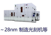
In one of the pictures, they refer to a 28nm litho machine that uses their anti-vibration system: it is visible the brand (a bit blurred), is a SMEE machine!

Untitled.png
 

tokenanalyst

Brigadier
Registered Member
For the record, the guy who is talking is from Huazhong University of Science and Technology (HUST) and it seems thay developed an active anti-vibration platform for lithographic machines.

This conference was held in July this year (so already half year ago).

In one of the pictures, they refer to a 28nm litho machine that uses their anti-vibration system: it is visible the brand (a bit blurred), is a SMEE machine!

View attachment 141923
At first I thought they used a photo of SMEE FPD machines but there none that looks like this one.

1735323964234.png 1735323990547.png
1735324011320.png
 

tokenanalyst

Brigadier
Registered Member

Hua Hong Semiconductor's patent for "Method for reducing plasma damage of PECVD thin films" is published​


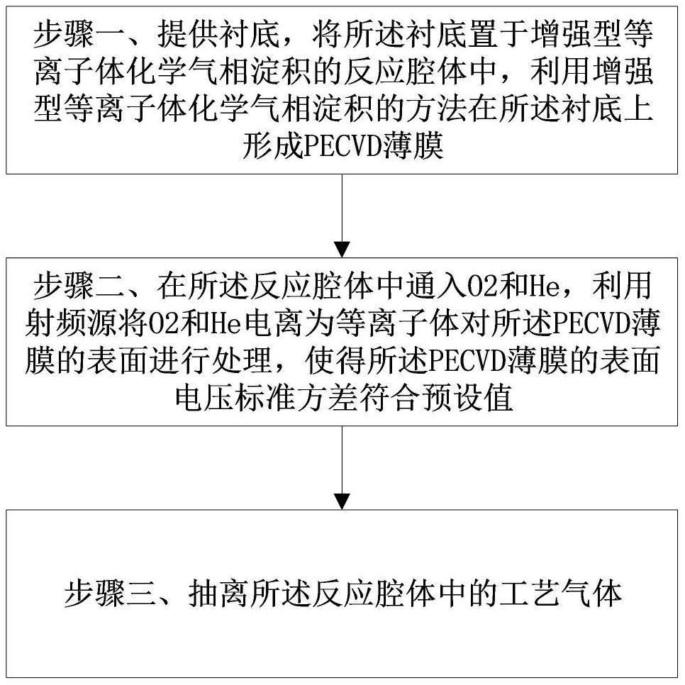
Tianyancha shows that Shanghai Huahong Grace Semiconductor Manufacturing Co., Ltd.'s patent for "Method for Reducing Plasma Damage to PECVD Thin Films" has been announced. The application publication date is November 15, 2024, and the application publication number is CN118957544A.
1378787329719.3416.png

The present invention provides a method for reducing plasma damage of PECVD thin film, providing a substrate, placing the substrate in a reaction chamber of enhanced plasma chemical vapor deposition, forming a PECVD thin film on the substrate by using the method of enhanced plasma chemical vapor deposition; introducing O2 and He into the reaction chamber, using a radio frequency source to ionize O2 and He into plasma to process the surface of the PECVD thin film, so that the surface voltage standard deviation of the PECVD thin film meets a preset value; removing the process gas in the reaction chamber. The present invention can significantly reduce the surface voltage standard deviation (Vs stdev) that finally characterizes the plasma damage trend.

Please, Log in or Register to view URLs content!
 

SanWenYu

Captain
Registered Member
That is the EUV. Have you noticed that the corresponding shock absorption modules above the other three devices are all physical photos, while only the shock absorption module corresponding to the EUV is a 3D model?
You are right. That 3D model is also shown in the next slide although from a different angle.
 
Top