Chinese semiconductor thread II

tokenanalyst

Brigadier
Registered Member
ASML CEO: "The restrictive policies of Western governments are compelling China to become highly innovative."
TSMC Executive: "The Americans and Europeans are underestimating China, but people should never underestimate China,"
MIPS founder back in 2019: "The harder we squeeze on export controls the more/faster China will innovate, acquire, copy, and steal"

Think Tanker with an Art Degree: Export Controls are effective.
Think Tanker with an History Degree: Export Controls are effective.
Chip Stock Guru: Export Controls are effective even if my stocks portfolio is collapsing in value due companies exposure to China.
D.C. Politician: Export Controls are effective even if reality says otherwise, is costing US companies billions, is costing US high paying jobs, is creating unwanted competition for US companies, destroy the already fragile commercial relationship with a mayor power, strain the relationship with our allies, we have to constantly close loopholes and there is no way to enforce the rules.
 

tokenanalyst

Brigadier
Registered Member

Important progress has been made in low-cost MOSFET based on new SiC composite substrate​


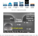
Recently, Liu Xinyu's team from the High Frequency and High Voltage Center of the Institute of Microelectronics, in collaboration with Qinghe Jingyuan Company, Nanjing Institute of Electronic Devices and other teams, successfully realized high-performance and low-cost 1200V SiC MOSFET based on a new 6-inch SiC composite substrate.
Currently, the silicon carbide (SiC) wafer industry is continuing to expand production capacity to meet growing market demand. However, the yield of defect-free substrates (i.e., "high-quality" substrates) that can be used for MOSFET manufacturing is typically only 40%-60%. During the growth and purification process of 6-8 inch SiC, low-grade substrates (i.e., "low-quality" substrates) are naturally produced. In current industrial production, these substrates are usually treated as companion wafers or even waste, resulting in high production costs for high-quality SiC substrates, which usually account for more than 50% of the cost of the final MOSFET device. In addition, the manufacturing process of SiC substrates consumes a lot of energy, resulting in higher carbon emissions.
To meet this challenge, the Institute of Microelectronics and its partners proposed a new type of 6-inch single-crystal SiC composite substrate for the first time in the world. Through surface activation bonding technology and ion implantation stripping technology, high-quality SiC thin layers were bonded and transferred to low-quality single-crystal SiC substrates, achieving effective use of low-quality single-crystal SiC substrates. Each high-quality SiC wafer can be reused more than 30 times (that is, each high-quality wafer can produce more than 30 thin layers), and the cost is expected to be reduced by 40%.
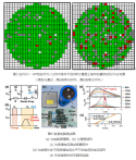
The composite substrate exhibits a defect density comparable to that of high-quality substrates, with an interface thermal resistance as low as 2.8 +1.4/-0.7 m²K/GW, and a very low electric field strength at the bonding interface. This interface thermal resistance is the lowest value reported internationally for bonding interfaces between SiC and other materials (such as SiC, GaN and Ga 2 O 3 ). The 6-inch SiC epitaxial layer grown on this substrate achieved a yield of up to 99.2% without fatal defects. The 1200V, 20mΩ SiC MOSFET device manufactured based on this 6-inch epitaxial layer demonstrated a yield of more than 70% (tested at I DSS <2µA, at 1200V), and its performance and reliability are comparable to the most advanced commercial devices. Circuit robustness testing showed that there was no degradation of the bonding interface under surge currents exceeding 250A and lasting 10ms. This achievement is the first report of wafer-level device data and high current robustness based on SiC composite substrates. The results show that this new substrate technology has great potential and provides an important development direction for more economical and sustainable SiC power electronics.

1735155735176.png1735155780288.png

Please, Log in or Register to view URLs content!
 

tokenanalyst

Brigadier
Registered Member

A novel Ω-SOI Gate-All-Around FET with doping free load-Si and two-step wet etching achieving superior leakage suppression and short-channel effects immunity​


Institute of Microelectronics, Chinese Academy of Sciences, Beijing.​

Abstract​

In this article, we proposed a novel 4-layer silicon-on-insulator (SOI) nanosheet (NS) Gate-All-Around (GAA) field-effect transistor (FET) with an Ω-structure (Ω-SOI). Through high-quality SiGe/Si multilayers epitaxy on the ground-plane (GP) doping free load-Si, and a two-step wet etching Ω-structure formation process, this novel Ω-SOI GAAFET was successfully fabricated, achieving threshold swing (SS), off-state current (Ioff), current ratio (Ion/Ioff), and drain-induced barrier lowering (DIBL) values of 65 mV/dec, 2.8 × 10⁻⁴ μA/μm, 3 × 10⁶, and 7 mV/V, respectively. Moreover, 3D technology computer-aided design (TCAD) simulation was applied in advanced node, confirming that this novel Ω-SOI GAAFET can provide enhanced gate control capability than conventional SOI (C-SOI) GAAFET, leading to superior leakage suppression, and short-channel effects (SCE) immunity. This novel Ω-SOI GAAFET is compatible with the process flow of mainstream GAAFET, providing a promising candidate for extending CMOS technology.​

Please, Log in or Register to view URLs content!
 

tphuang

Lieutenant General
Staff member
Super Moderator
VIP Professional
Registered Member
SMIC's 28nm process price has dropped sharply from $5,000 to $1,500.

Please, Log in or Register to view URLs content!
I do think this is unlikely since we haven’t seen any major declines in SMIC ASP overall. It’s just too hard for 28nm to drop this much without being noticed. Although I am sure it has dropped a lot for the commoditized types like DDIC driver
 
Top