How much is the H100?That actually would be a disappointment. Where did you get the computation figures?
You are using an out of date browser. It may not display this or other websites correctly.
You should upgrade or use an alternative browser.
You should upgrade or use an alternative browser.
Chinese semiconductor thread II
- Thread starter vincent
- Start date
910C is just 2 improved 910B(320TFLOP) dies joined together like BlackwellThat actually would be a disappointment. Where did you get the computation figures?
The actual performance is 800 TFLOPS(2 dies at 400 TFLOPS each) at FP16
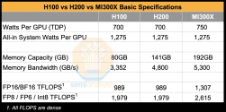
989 TFLOPS at FP16How much is the H100?
Interconnect speed is the bigger problem
910C is just a stopgap for Huawei
Ascend 920/910D is the real deal
It will be on SMIC N+2 and interconnect speed will be more than 1Tbps
Single-die performance will match H100
While the chip as a whole(2 dies joined together like in Blackwell) will match B200
A simple google will indicate H100 does more computation than that for FP16.910C is just 2 improved 910B(320TFLOP) dies joined together like Blackwell
The actual performance is 800 TFLOPS(2 dies at 400 TFLOPS each) at FP16
989 TFLOPS at FP16
Interconnect speed is the bigger problem
910C is just a stopgap for Huawei
Ascend 920/910D is the real deal
It will be on SMIC N+2 and interconnect speed will be more than 1Tbps
Single-die performance will match H100
While the chip as a whole(2 dies joined together like in Blackwell) will match B200
If you have proof that 910C is two 910B die stitched together, then please provide that.
Nvidia intentionally uses the sparsity enabled performance in their official press releaseA simple google will indicate H100 does more computation than that for FP16.
Nobody uses this configuration for training or inference
I'm talking about dense performance


The picture @olalavn posted literally has 2 dies stitched together like in Blackwell or Apple M seriesIf you have proof that 910C is two 910B die stitched together, then please provide that.
Kirin PC chip will also be like that
Nvidia intentionally uses the sparsity enabled performance in their official press release
Nobody uses this configuration for training or inference
I'm talking about dense performance
That’s fine. State it as such.
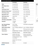
That’s fine. Nobody is doubting that 910C use two dies. What I am asking for is proof that it is using two 910B. You are telling me they spend 2 years and haven’t added more computation density.View attachment 141467
View attachment 141466
The picture @olalavn posted literally has 2 dies stitched together like in Blackwell or Apple M series
Kirin PC chip will also be like that
80 TFLOP improvement(25% more performance) on each dieYou are telling me they spend 2 years and haven’t added more computation density.
Each die on Blackwell also has a 25% compute improvement compared to H100
Ascend 910B/C is on SMIC N+1
Adding more transistors would have led to worse yields
As I said before 910C is a stopgap
They learned how to stitch together dies through high-bandwidth fabric
Most of their time was spent on Ascend 920 and improving interconnect speed
U will see all the GPU innovation that Huawei has developed after being sanctioned on Ascend 920(late 2025)
Huawei will remain 1 generation behind Nvidia until they can fab on EUV
Last edited:
I do think this is unlikely since we haven’t seen any major declines in SMIC ASP overall. It’s just too hard for 28nm to drop this much without being noticed. Although I am sure it has dropped a lot for the commoditized types like DDIC driver
What do you expect when it's written by some blogger named Little Drawing Fairy? People should refrain from posting stuff from random nobodies.
it's just a test version of the SMIC process, it's also a low power version but it's not a high performance version yet.... 910D coming next year will have a different lookThat actually would be a disappointment. Where did you get the computation figures?
So basically, there is absolutely no proof.80 TFLOP improvement(25% more performance) on each die
Each die on Blackwell also has a 25% compute improvement compared to H100
Ascend 910B/C is on SMIC N+1
Adding more transistors would have led to worse yields
As I said before 910C is a stopgap
They learned how to stitch together dies through high-bandwidth fabric
Most of their time was spent on Ascend 920 and improving interconnect speed
U will see all the GPU innovation that Huawei has developed after being sanctioned on Ascend 920(late 2025)
Huawei will remain 1 generation behind Nvidia until they can fab on EUV
910B is already at 320 TFLOPS.
as for the rest, I have already explained recently. The majority of ascend dies produced in this past year have been at TSMC with N7 process.
