Chinese semiconductor thread II

JPaladin32

New Member
Registered Member
Actually, digging out some notes I had when 9000s first came out, I'm now confused by why Techinsights claimed "no change in process". The dimensions of 9000s process are:

CPP: 63nm, fin pitch: 33nm, metal pitch: 42nm

Now, I see some reports say that the dimensions of 9020 are:

CPP: 63nm, fin pitch: 31nm, metal pitch: 40nm

So, there is a reduction of transistor dimensions here. But, maybe they just feel these reductions are too incremental to call a "change in process". But anyway, these dimensions are still in 7nm territory, so it's fair to still call it N+2 and nothing more.
 

tokenanalyst

Brigadier
Registered Member

North Huachuang: Plans to participate in the establishment of Beijing Integrated Circuit Equipment Industry Investment and M&A Phase II Fund​


On December 16, North Huachuang announced that it plans to use its wholly-owned subsidiary Huachuang Venture Capital as an investment platform, and jointly establish Beijing Integrated Circuit Equipment Industry Investment and M&A Phase II Fund (Limited Partnership) (hereinafter referred to as "Phase II Fund") with partners such as Beijing Electric Control Industry Investment Co., Ltd. and Beijing State-owned Capital Operation Management Co., Ltd. The total fundraising scale of Phase II Fund is 3 billion yuan.
The first phase of the fund raising plan is no more than 2.5 billion yuan in cash, of which Huachuang Venture Capital plans to subscribe 510 million yuan. The second phase of the fund will mainly invest in the semiconductor field through mergers and acquisitions and equity investments, focusing on equipment, parts, materials, software, components and upstream and downstream new technologies, new materials, and new applications.
In addition, in the first phase of fundraising, Beijing Guoguan plans to subscribe 500 million yuan; the fund managed by Beijing Yizhuang International Industrial Investment Management Co., Ltd. plans to subscribe 500 million yuan; the fund managed by Beijing Zhongguancun Capital Fund Management Co., Ltd. plans to subscribe 500 million yuan; Electric Control Industrial Investment plans to subscribe 200 million yuan; Shanghai Pudong Leading Area Guotai Junan Science and Technology Innovation No. 1 Private Equity Fund Partnership (Limited Partnership) plans to subscribe 100 million yuan; Shanghai Lingang Guotai Junan Technology Frontier Industry Private Equity Fund Partnership (Limited Partnership) plans to subscribe 100 million yuan; CITIC Construction Investment Co., Ltd. plans to subscribe 60 million yuan; Beijing Novartis Capital Investment Management Co., Ltd. plans to subscribe 30 million yuan; the remaining 500 million yuan of capital is planned to be raised by the fund manager Novartis through capital marketization.

Please, Log in or Register to view URLs content!
 

tphuang

Lieutenant General
Staff member
Super Moderator
VIP Professional
Registered Member
Actually, digging out some notes I had when 9000s first came out, I'm now confused by why Techinsights claimed "no change in process". The dimensions of 9000s process are:

CPP: 63nm, fin pitch: 33nm, metal pitch: 42nm

Now, I see some reports say that the dimensions of 9020 are:

CPP: 63nm, fin pitch: 31nm, metal pitch: 40nm

So, there is a reduction of transistor dimensions here. But, maybe they just feel these reductions are too incremental to call a "change in process". But anyway, these dimensions are still in 7nm territory, so it's fair to still call it N+2 and nothing more.
I'm waiting for the feature sizes to come out on 9020. But if it does have metal pitch of 40nm and fin pitch of 31nm, this confirms what hvpc said a while back. It's all within realm of possibilities. This basically means a small increase in transistor density and hopefully just general improvements in how well the chip is made, which explains the lower power consumption in 9020 vs 9000S.

At end of the day, I was never expecting N5 type of density this year (or even 2025 tbh). I was expecting 10 to 20% increase in transistor density depending on whether they achieved 38 vs 40nm metal pitch.

Steady improvement is the likely outcome until whenever EUV is available.
According to available information, the cost to build a SMIC 14nm fab is estimated to be around $8.87 billion. This figure comes from reports about a "GigaFab" project by SMIC, which is designed to produce 14nm chips and is estimated to cost nearly $8.87 billion

So India's 65nm for $11 billion is costly. more costly than SMIC's 14nm fab.

My educated estimate for China's 65nm Fab is $3 to $5billion.
Right, all of this is fine. No one is questioning that it's a lot cheaper to build things in China. But for accuracy, let's try to compare apples to apples.
 

OppositeDay

Senior Member
Registered Member
Are sk or Samsung producing ddr5 die in their Chinese fabs?

I don’t think they use EUV, so not sure they ever tried ddr5 in china

In Chinese colloquial linguistic context '国产' without any further qualifications means produced in China by a Chinese company. Glowy generally specifies the die manufacturer for each of their product. Since this particular product only says it's 国产 without specifing manufacturer it's reasonable to assume it's CXMT. Let's wait for reviews.
 
Last edited:

tokenanalyst

Brigadier
Registered Member

Another CMP polishing liquid project was successfully signed​


Semiconductor wafer CMP polishing liquid is one of the key materials in the semiconductor manufacturing process and plays a vital role in improving the flatness and smoothness of the wafer surface.

Li Yongxiu, Dean of the Rare Earth Research Institute of Nanchang University, and Yuan Ye, General Manager of Ruisibo, jointly signed a cooperation agreement on the CMP polishing liquid project. The successful signing of the project has laid a solid foundation for the cooperation between the two parties. The cooperation between Ruisibo and Nanchang University will give full play to the advantages of both parties, strengthen cooperation in technology research and development, talent training, etc., promote the development of the CMP polishing liquid project, and improve China's independent innovation capabilities and market competitiveness of semiconductor materials.

Please, Log in or Register to view URLs content!
 

tokenanalyst

Brigadier
Registered Member

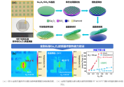
CAS achieves breakthrough in diamond-based gallium oxide heterogeneous integrated materials and devices​


A team from the Shanghai Institute of Microsystem and Information Technology, Chinese Academy of Sciences, and a team from the Nanjing Institute of Electronic Devices have made breakthrough progress in the field of diamond-based gallium oxide heterogeneous integrated materials and devices.
According to the official WeChat account of the Shanghai Institute of Microsystem and Information Technology, Chinese Academy of Sciences, the Shanghai Institute of Microsystem and Information Technology's heterogeneous integration XOI team and the Nanjing Institute of Electronic Devices' ultra-wide bandgap semiconductor research team have collaborated to achieve breakthrough progress in the field of diamond-based gallium oxide heterogeneous integrated materials and devices.

1734393035832.png


This research work fully proves that wafer-level diamond-based gallium oxide heterogeneous integrated materials have excellent heat dissipation capabilities and RF application prospects. It is another major breakthrough after silicon-based and silicon carbide-based gallium oxide heterogeneous integrated materials. It will further promote the development of high-performance gallium oxide devices and provide a new paradigm for the preparation of diamond-based heterogeneous integrated materials.

Please, Log in or Register to view URLs content!
 

tphuang

Lieutenant General
Staff member
Super Moderator
VIP Professional
Registered Member

CAS achieves breakthrough in diamond-based gallium oxide heterogeneous integrated materials and devices​


A team from the Shanghai Institute of Microsystem and Information Technology, Chinese Academy of Sciences, and a team from the Nanjing Institute of Electronic Devices have made breakthrough progress in the field of diamond-based gallium oxide heterogeneous integrated materials and devices.
According to the official WeChat account of the Shanghai Institute of Microsystem and Information Technology, Chinese Academy of Sciences, the Shanghai Institute of Microsystem and Information Technology's heterogeneous integration XOI team and the Nanjing Institute of Electronic Devices' ultra-wide bandgap semiconductor research team have collaborated to achieve breakthrough progress in the field of diamond-based gallium oxide heterogeneous integrated materials and devices.

View attachment 141009


This research work fully proves that wafer-level diamond-based gallium oxide heterogeneous integrated materials have excellent heat dissipation capabilities and RF application prospects. It is another major breakthrough after silicon-based and silicon carbide-based gallium oxide heterogeneous integrated materials. It will further promote the development of high-performance gallium oxide devices and provide a new paradigm for the preparation of diamond-based heterogeneous integrated materials.

Please, Log in or Register to view URLs content!

this is unreal here. Look at that power to temperature ratio. It's hard to imagine a better radar material than this for the next decade.

With this type of RF, they can presumably use it for other power applications too.

Do people realize what we are looking at here?

looks like 南京电子器件研究所 is CETC 55th institute, which does a lot of the power/RF semiconductor research.
 
Last edited:

tphuang

Lieutenant General
Staff member
Super Moderator
VIP Professional
Registered Member
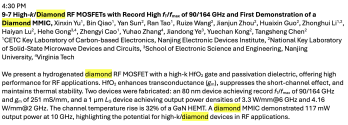
so this was presented at IEDM 2024 where the highlight was TSMC presenting 2nm wafer technology.

I don't really care much about that, so I looked down on the program on diamond related stuff

Please, Log in or Register to view URLs content!
Screenshot 2024-12-16 at 9.44.54 PM.png

so the section after the one we discussed was also diamond related from basically the same people.

Note that they created diamond MMIC with 117mW output power at 10GHz. Again, this indicates using Diamond with GaN? you can get temperature rise down by quite a bit vs your standard GaN HEMT, which allows for this high power RF MMIC.
 

tphuang

Lieutenant General
Staff member
Super Moderator
VIP Professional
Registered Member
and then I looked at the other RF presentation from that day.
Screenshot 2024-12-16 at 9.51.03 PM.png
You will see that all these American research. None of them are using Diamond at all. Most of this is just GaN on other substrate or other type of technology.

It seems like China is the only one making progress here on diamond substrate
 
Top