Chinese semiconductor thread II

tokenanalyst

Brigadier
Registered Member

A novel wavefront modulation approach in the extreme ultraviolet.​


Zhejiang Univ.
China Jiliang Univ.

Abstract​

In recent years, the application of Extreme Ultraviolet (EUV) technology has been expanding rapidly across various fields, particularly in lithography, nanoscale imaging, and spectroscopy. Metasurfaces, on the other hand, offer a promising route for miniaturized and lightweight optical devices, with the potential to become one of the directions for future EUV device advancements.

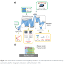
In this study, we present a design for a transmissive phase-type metasurface lens for EUV photolithography. After careful consideration of various materials and pore shapes, we selected molybdenum as the optimal substrate material due to its superior optical properties in the EUV range. Finally, we achieved 2π phase modulation while maintaining high transmittance through a patterned vacuum-guided approach, enabling high-precision wavefront modulation. This choice maximizes the performance and efficiency of the metasurface in the EUV regime.

Numerical simulations demonstrate that the metasurface lens exhibits excellent optical performance. Our findings contribute to the ongoing exploration of photolithography and hold potential for transforming future EUV technologies, particularly in applications requiring high-precision optical components​

Please, Log in or Register to view URLs content!
 

tokenanalyst

Brigadier
Registered Member

Probability distribution-based method for aberration budgeting in EUV lithography.​

Abstract​


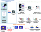
Extreme ultraviolet (EUV) lithography is one of the most indispensable technologies in semiconductor manufacturing for 7 nm and smaller technology nodes. However, many key parameters in the lithography system may deviate from target values, and there are extremely complex coupling effects among these parameters. Additionally, aberrations that far exceed expectations damage lithography results severely. These accidents pose significant challenges in achieving satisfactory lithography outcomes. To investigate the impact of aberrations coupled with multiple key parameters on lithography results, and to provide quantitative and precise direction for the research and development of lithography systems, this paper proposes a methodology of budget analysis of aberrations based on probability distribution. First, a rapid prediction model of lithography results is established by multilayer perceptron. Then, the lithography results under different parameter conditions are obtained according to the prediction model. Subsequently, the aberration combinations that meet lithography requirements are filtered out. Finally, the impact of each aberration on lithography results and their budget range can be determined according to the general distribution and joint probability distribution of aberrations coupled with multiple key parameters. For patterns commonly used in EUV single exposure at the 5 nm technology node, this paper finds that aberrations such as Z2 and Z4 exhibit significant impacts on lithography results under the coupling of multiple key parameters. Additionally, all the budget ranges of aberrations are obtained. Specifically, for example, Z2, Z4, and Z5, their budget ranges are -18∼15mλ, 10∼45mλ, 7∼43mλ, respectively. While items such as Z1 and Z27, their budget ranges are -40∼40mλ consistently. This method can obtain the impact and budget range of aberrations under the coupling of multiple key parameters in the lithography system quickly and accurately. It can provide a reliable guideline for aberration compensation and optimization, and the research and development of lithography systems. Moreover, the budget ranges obtained by this method can also serve as a clear indicator for aberration monitoring.

1732567834117.png1732567901373.png

Please, Log in or Register to view URLs content!
 

tokenanalyst

Brigadier
Registered Member

Semiconductor equipment (Wet Processing) and CMP consumables manufacturer GMC is rushing to go public!​


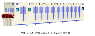
GMS Semiconductor Technology (Wuxi) Co., Ltd. completed the registration for tutoring with the Jiangsu Securities Regulatory Bureau, and CITIC Securities served as the tutoring institution for GMS's initial public offering. Source of Jimsi filing report: Advanced Semiconductor Materials GMC: China's leading semiconductor equipment platform company GMC Semiconductor Technology (Wuxi) Co., Ltd. was established in 2014.

Initially, it mainly provided refurbishment services for semiconductor equipment and spare parts of foreign brands. For example, the company's refurbished equipment covers most of the semiconductor front-end processes, such as chemical mechanical polishing equipment and dry etching equipment. At the same time, GMC has also continuously expanded its own brand product line, striving to gain a foothold in the market.

After several years of development, GMS has now become a major supplier of 6-inch, 8-inch and 12-inch wafer equipment and process solutions, and is a leading domestic semiconductor equipment platform company. The company is currently mainly engaged in the research and development, manufacturing, sales and services of various semiconductor process equipment, process auxiliary equipment, CMP consumables, etc. It is committed to providing high-quality and cost-effective equipment, materials and services, cultivating excellent semiconductor equipment and process R&D talents and teams, helping the progress and upgrading of China's semiconductor industry, and promoting the progress of human science and technology.
1732571608594.png


With a strong localized engineering team and independent innovation capabilities, GMC has provided customized equipment and process solutions for more than 100 wafer fabs including SMIC and HHGRACE. Its outstanding performance and services have won wide recognition in the market. The total number of employees has exceeded 1,400, the plant area has reached 165,000 square meters, and sales revenue is expected to reach 1.2 billion yuan in 2024.​

Please, Log in or Register to view URLs content!
 

tokenanalyst

Brigadier
Registered Member

Zhongke Jinci accelerates the development of semiconductor equipment precision ceramic parts.​


Zhongke Jinci completed a PreA round of capital increase of tens of millions of yuan. This round of financing will be used to further enhance the company's development capabilities of precision ceramic components technology. China Powder Network reported that recently, Shenyang Industrial Technology Research Institute system company Shengke Venture Capital and other social capital completed the PreA round of capital increase of tens of millions of yuan for Zhongke Jinci. This round of financing will be used to further enhance the company's development capabilities of precision ceramic parts technology, promote new product development and standardized production of mass-produced products . In addition, Zhongke Jinci has completed the registration of its Shenyang industrialization subsidiary, which is located in Shenyang Aviation Industry Park. In the future, it will gradually build production lines and carry out localized production.

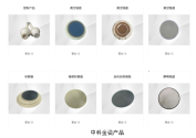
Zhongke Jinci: A newcomer in the production of precision ceramic parts Founded in April 2023 and headquartered in Ningbo, Zhongke Jinci is focused on the research and development and industrialization of new semiconductor process ceramic materials and related components such as wafer electrostatic chucks and ceramic heating plates. It has full-process technology and manufacturing capabilities for special ceramics and ceramic-based electronic components from raw material synthesis and processing, powder production, precision molding, sintering, precision and ultra-high precision processing and functional processing.

1732572420056.png

Please, Log in or Register to view URLs content!
 

ansy1968

Brigadier
Registered Member
"Xiaomi Will ‘Officially Unveil’ Its Custom 3nm Chipset Next Year, With A Report Stating That The Silicon Will Be Positioned To Replace Qualcomm And MediaTek"

Please, Log in or Register to view URLs content!


Please, Log in or Register to view URLs content!
Well and good BUT who will FAB it TSMC? They seems very confident to official announce it like this not worrying what Qualcomm would do to sabotage this plan especially with Trump hawkish stance against anything Chinese.
 

tokenanalyst

Brigadier
Registered Member

GalaxyCore Announces Successful Mass Production of Multispectral CIS​

GalaxyCore announced the successful mass production of multispectral CIS, giving new capabilities to image sensors. This solution can accurately identify spectral information in scenes under complex ambient light, improve color reproduction capabilities, and enable more intelligent detection applications to meet consumers' more intelligent and refined needs.

Not long ago, GalaxyCore announced in an institutional survey that the company's 50-megapixel image sensor products have been mass-produced and shipped. The product is based on the single-chip high-pixel CIS architecture of GalaxyCore's 32-megapixel image sensor, which has been mass-produced. Through the unique FPPI technology and innovative circuit design, logic and pixel wafer manufacturing are realized on the same layer, and finally only one effective wafer is needed to realize high-pixel and high-performance products.
GalaxyCore said that its 50-megapixel image sensor has excellent color reproduction performance and provides excellent image resolution. The precise phase focus technology can quickly capture high-dynamic images, providing a differentiated high-pixel solution for the rear main camera of mainstream mobile phones.

According to reports, GalaxyCore's 50-megapixel image sensor has successfully entered the rear main camera market of mid-to-high-end brand mobile phones at home and abroad. It said that this marks that the company's innovative single-chip high-pixel chip integration technology has been further recognized by the market. In the future, the company will further iterate the performance of high-pixel products and launch higher-pixel products based on high-pixel single-chip integration technology, continuously enhance the company's core competitiveness, increase market share, and expand its leading advantage.

Please, Log in or Register to view URLs content!
 

tokenanalyst

Brigadier
Registered Member

Zhongke Xinyuan: A pioneer in domestic thermoelectric temperature control equipment, filling the technological gap​


Zhongke Xinyuan is the first company in China to achieve large-scale application of high-power semiconductor temperature control technology. Its products are widely used in many high-tech fields such as semiconductors, communications, computing equipment, medical care and new energy vehicles.

Zhongke Xinyuan's "star product" semiconductor direct cooling machine stands out among many products with its compact design, precise temperature control capability, fast response time, low energy consumption and no noise pollution. It can not only significantly reduce the cost of electricity consumption, but also completely eliminates the need to use harmful substances such as Freon, which perfectly meets the requirements of today's society for green and environmentally friendly development.

With continuous technological exploration and market development, Zhongke Xinyuan has obtained 10 invention patents, 27 utility model patents and 3 design patents, and won the 2023 China Semiconductor Investment Alliance's Annual Technology Breakthrough Award and the 2024 SSMC's Green Supply Chain Strategic Partner Award. Zhongke Xinyuan's core technology has not only broken the foreign technology monopoly in the domestic market, but has also served well-known companies such as TSMC, Huahong Grace, Silan Microelectronics, Innoscience, and Star Semiconductor, and has been exported to international markets such as the United States, Europe, Singapore, and Malaysia, serving SSMC, Infineon, STMicro, GlobalFoundries, SilTerra, PSK and other customers.


Please, Log in or Register to view URLs content!
 
Top