Chinese semiconductor thread II

tonyget

Senior Member
Registered Member

BYD co-developed the current industry's best auto cockpit SoC with the help of Mediatek using N4 process.

Seem to be consistent with this article


Please, Log in or Register to view URLs content!
对于中国大陆的AI芯片厂商来说,接下来芯片的代工,将成为需要解决的首要问题。
除了向大陆代工厂转单外,也有厂商选择与国外厂商合作的方式来绕过监管。比如某互联网大厂在自研AI芯片时,就选择与博通联合研发,两者合作开发的芯片最终可能交由英特尔代工。
For AI chip manufacturers in mainland China, chip foundry will become the primary issue that needs to be resolved.
In addition to transferring orders to mainland foundries, some manufacturers also choose to cooperate with foreign manufacturers to bypass supervision. For example, when a large Internet company was developing its own AI chip, it chose to jointly develop it with Broadcom. The chip jointly developed by the two may eventually be outsourced to Intel.
 

tokenanalyst

Brigadier
Registered Member

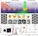
Hefei Research Institute and others efficiently construct gold microsphere array heterogeneous conductive adhesive for advanced packaging.​


Recently, the Nanomaterials and Device Technology Research Department of the Institute of Solid State Engineering, Hefei Institutes of Physical Science, Chinese Academy of Sciences, in cooperation with the Polymer and Composite Materials Research Department, Guangdong, Hong Kong and Macao Quantum Science Center, etc., has made new progress in the rapid preparation and performance research of heterogeneous conductive gold microsphere arrays , and achieved the efficient construction of heterogeneous conductive adhesives for advanced packaging of gold microsphere arrays. The relevant research results were published in Nature Communications .

Arrayed anisotropic conductive paste (ACF) is a method of configuring conductive microsphere particles in an array on a cross-linked polymer layer. It can effectively solve the problems of random distribution of particles in traditional ACF, leading to lateral short circuits, and ensure more reliable electrical connection. It is a new paradigm for ultra-high density packaging. In 2014, Dexerials Corporation of Japan used metal-plated polymer microspheres as conductive particles and arranged them in a precise array, realizing the commercialization of arrayed ACF for the first time.

However, due to the weak bonding between the metal shell and the polymer, this type of conductive particle faces challenges in bonding under actual deep pressing, which can cause the metal shell to break and detach, affecting the overall conductive performance.

In contrast, ordered arrays of pure metal microspheres, due to their inherent ductility, can theoretically ensure excellent electrical conductivity even under deep lamination, making them ideal next-generation packaging materials. However, due to the limitations of the anisotropic growth law of metals, the large-scale preparation of micron-scale pure metal spheres and their array arrangement has always been a challenging problem in the industry.

In response to the above problems, the researchers developed a simple, fast and efficient strategy based on the positioning transient emulsion self-assembly method proposed by the team in the early stage, combined with nanosecond laser pulse irradiation technology, to achieve the rapid preparation of a new pure gold microsphere array with uniform size, smooth surface and accurate positioning (Figure 1). This strategy effectively breaks the inertial thinking of "synthesis first and then positioning" in ACF product manufacturing, and provides a new solution for the rapid construction of arrayed ACF.

The key to this strategy is to use the laser-induced rapid layer-by-layer melting-fusion process to effectively avoid the anisotropic growth of the metal. Theoretical simulations have found that this layer-by-layer melting-fusion is mainly due to the limited skin depth of the laser, which localizes the photothermal effect generated by the gold particles on the surface of the superparticles. In addition, this method is highly universal and suitable for various nanoparticles with strong photothermal effects as assembly primitives, regardless of their size, morphology and composition. For example, the researchers used Au-Pd and Au-Ag-Pt core-shell nanoparticles as assembly primitives to prepare Au-Ag-Pd-Pt alloy microspheres with uniform size and smooth surface (Figure 2), which are expected to be used in the efficient preparation of high-entropy alloy microspheres with uniform particle size.

Compared with commercial gold-plated microspheres, the pure metal microspheres benefit from the excellent ductility and plasticity of pure gold materials, showing ultra-stable conductive properties under deep compression (Figure 3). The pure gold microsphere array is expected to provide the best solution for ultra-high-density bonding of micro-display μLED chips , thereby promoting the development and application in the field of high-resolution display.
1732544923164.png

Please, Log in or Register to view URLs content!
 

tphuang

Lieutenant General
Staff member
Super Moderator
VIP Professional
Registered Member
Seem to be consistent with this article


Please, Log in or Register to view URLs content!
BYD doesn't have enough experience with chip design to do it on its own. However, it does have a design team and can do testing and packaging. So it can take Mediatek design and do some modification, put a batch on it. And get it fabb'd and received for a lower price.
This also allows it to gain some experience and actually design its own lower end Cockpit chip in the future.
 

tokenanalyst

Brigadier
Registered Member

Total investment of 2.5 billion! Xiangxin Semiconductor Production Base (Phase I) project started​


The groundbreaking ceremony for the Xiangxin Semiconductor Production Base (Phase I) project was held in Louxing Industrial Development Zone.
The Xiangxin Semiconductor Production Base (Phase I) project is one of the important achievements of Loudi's 100-day project construction campaign and the "three-electric" industry investment promotion "double hundred" campaign, and is an important supporting project of the AIPER "1+N" intelligent manufacturing industrial park. After the project reaches full production, it will have an annual production capacity of 30,000 core components for semiconductor equipment, and will build my country's first large-size electrostatic chuck production line, silicon carbide etching ring production line, and magnetic levitation molecular pump production line.

Please, Log in or Register to view URLs content!
 

tphuang

Lieutenant General
Staff member
Super Moderator
VIP Professional
Registered Member
From Huawei whisper on M70

听说这次华为Mate70系列备货很充足,但是也有很大可能供不应求,特别是Pro+和非凡大师版本,这两个版本因为制造工艺和价格,前期不太敢放开量备货,但是也比去年多一些。不过按华为的热度,我觉得就算华为准备500万的前期货也不够抢的
[笑cry]
[笑cry]
[笑cry]


Please, Log in or Register to view URLs content!
Note the wording on here, plenty of supply, but certain models like Pro+ and RS model may not have enough stock due to the extra manufacturing workmanship involved.
He feels like Huawei may have 5 million ready already.

What does this mean? Ignore the nonsense out there about yield on N+3 being too low.
Clearly, there is no supply issue with Kirin-9100
Any supply issue will be caused by other production/supply chain factors.
Also, no issue with any other part of Huawei's supply chain including YMTC NAND, CMOS chips, RF chips and all the analog chips. Huawei has fully developed a chip supply chain domestically able to support flagship phone
 

tphuang

Lieutenant General
Staff member
Super Moderator
VIP Professional
Registered Member
View attachment 140015
CIOMP LPP EUV laser patent was authorized.

View attachment 140016
OMG, look at the date on that. So their LPP EUV laser was already developed 2 years ago. That made all the sense in the world for the news last year of the EUV prototype that came out.
And then since that point, we see a steady drip of other patent which I imagine are things they got working after they started testing the prototype. Probably still a couple of years away from HVM.
 

tphuang

Lieutenant General
Staff member
Super Moderator
VIP Professional
Registered Member
BYD doesn't have enough experience with chip design to do it on its own. However, it does have a design team and can do testing and packaging. So it can take Mediatek design and do some modification, put a batch on it. And get it fabb'd and received for a lower price.
This also allows it to gain some experience and actually design its own lower end Cockpit chip in the future.
btw,
This in itself is a pretty exciting news from everyone around BYD.
I heard design to fab was done record time. Nobody in Mediatek work has ever seen anything like it.
With this first high end cockpit SoC designed, it seems reasonable that their next steps are to design lower end cockpit chip by themselves as well as high end MCUs. This showcases BYD has a decent chip design team already.

Cost wise. If you think about TSMC 4nm wafer probably costing $16k. If you get 500 good die from that, then even die is basically $32. If you add in royalty for Mediatek + memory, packaging, the other PCB, various analog chips and testing cost. You can have BYDE do a lot of that. You might be able to do the entire thing in like $100 per SoC.

That's a huge discount vs buying a high end SD8295 from Qualcomm which probably will cost $500.
 
Last edited:
Top