Chinese semiconductor thread II

tokenanalyst

Brigadier
Registered Member

Zhongke Feice: Bright field nano-pattern wafer defect inspection equipment has been shipped in small batches.​


the bright-field nano-pattern wafer defect detection equipment has been shipped in small batches; its dark-field nano-pattern wafer defect detection equipment has been shipped to some customers' production lines for process development and application verification; the optical critical dimension equipment currently has good verification results on the client side, and is undergoing corresponding testing for delivery to the customer's mass production department." In particular, the investment in bright-field and dark-field equipment is very large. The goal is to complete the verification of the equipment in the customer's production line as quickly as possible and complete localized replacement. "

Chen Lu added.Regarding the current market demand performance of the company's semiconductor quality control equipment, Gu Kainan, director and secretary of the board of directors of China Science and Technology Testing, said that benefiting from the continuous expansion of production capacity of domestic wafer fabs, the domestic semiconductor equipment industry is in a period of rapid development.It is worth mentioning that in recent years, applications such as AI and computing chips have brought many technological innovations to integrated circuit manufacturing, including 2.5D and 3D packaging used in HBM. These process innovations have also put forward higher requirements for detection and measurement equipment.


wafer defect detection tool:

1732371398521.png

CD measurement tool
1732371495867.png

Please, Log in or Register to view URLs content!
 

tokenanalyst

Brigadier
Registered Member

One of China biggest semiconductor testing lab is rising funds to expand.​


Shengke Nano intends to raise 297 million yuan to be used for the construction project of improving the testing and analysis capabilities in Suzhou.

Shengke Nano was established in 2012 and is a well-known third-party semiconductor testing and analysis laboratory in the industry. It provides sample failure analysis, material analysis, reliability analysis and other analytical experiments to customers across the entire semiconductor industry chain.

Sembcorp Nano's technical capabilities in the two more difficult business areas of semiconductor failure analysis and material analysis are comparable to those of leading companies in the industry, such as Hong Kang and CESI Labs, and it is in the leading or relatively advanced position in the indicators of many analysis projects. Sembcorp Nano's analytical capabilities can cover 3nm advanced processes, which is at the forefront of the industry.

Sembcorp Nano is one of the leading third-party laboratory companies in China. In 2023, Sembcorp Nano's domestic market share is about 4.23%, and its business scale is relatively advanced among the leading companies.
In the areas of failure analysis and material analysis, which are its main focus, Sembcorp Nano's domestic market share is approximately 7.86%. Especially in the failure analysis business, the company's sales revenue is ahead of its main competitors.In terms of market prospects, Shengke Nano said that with the development of the semiconductor industry, the efficient industry vertical division of labor model is becoming increasingly in-depth. Following Fabless, the Labless model of entrusting third-party laboratories to conduct testing has become a new industry development trend. In recent years, it has been increasingly sought after by the market and is also in line with the future mainstream development trend of the semiconductor industry.
Please, Log in or Register to view URLs content!
 

defect

New Member
Registered Member
For those chip on a wafer type "packages". How do you write on them? I mean, do you use masks? This maybe really good for imprint lithography. where you have a, "mask" the size of the wafer. But really interesting.

What is the biggest issue with these types of packages?
 

tokenanalyst

Brigadier
Registered Member
For those chip on a wafer type "packages". How do you write on them? I mean, do you use masks? This maybe really good for imprint lithography. where you have a, "mask" the size of the wafer. But really interesting.

What is the biggest issue with these types of packages?
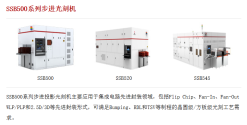
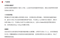
My guess that chips are patterned in the wafer and then send to a packaging facility to make the interconnects using I-line scanners but DUV scanners have a small FOV, so a packaging scanners like SMEE 500 series will be needed because have large patterning footprint.

1732374049122.png
1732374113758.png

Imprint lithography could be an option.
 

antwerpery

New Member
Registered Member
So how bad is the TSMC ban on advanced nodes is going to be for Chinese A.I development? EUV is many years away and I don't think SMIC can scale up 7nm/5nm fast enough to cover the needs of a very rapidly growing industry. The good news is that it's clear that LLM models are seeing diminishing returns and will likely hit a wall where throwing more processing power and data at it only results in negligible improvements meaning that America won't race nearly too much in A.I development while China is currently constrained on computing power.
 

tphuang

Lieutenant General
Staff member
Super Moderator
VIP Professional
Registered Member
So how bad is the TSMC ban on advanced nodes is going to be for Chinese A.I development? EUV is many years away and I don't think SMIC can scale up 7nm/5nm fast enough to cover the needs of a very rapidly growing industry. The good news is that it's clear that LLM models are seeing diminishing returns and will likely hit a wall where throwing more processing power and data at it only results in negligible improvements meaning that America won't race nearly too much in A.I development while China is currently constrained on computing power.
AI related stuff is in AI thread.

There is no shortage of AI chips in China if you looked through this thread. Please read up on this thread before asking questions like this.

H100 computing rental cost in China is lower than America. There is no shortage of H100 getting smuggled in.

I really hate to have to answer the same question all the time when you can just read up this thread.
 

FairAndUnbiased

Brigadier
Registered Member
Does CN mainland have local manufacturer of blank masks?

A DUV mask blank is a piece of glass with Cr coating. It is literally that simple. The Cr is patterned with maskless laser or ebeam lithography followed by chemical etching. That is actual mask production, which is quite a bit harder than PVD of Cr on glass.

EUV mask blank are complex Mo/Si multilayers but they aren't what SK is selling.
 

gelgoog

Lieutenant General
Registered Member
So how bad is the TSMC ban on advanced nodes is going to be for Chinese A.I development? EUV is many years away and I don't think SMIC can scale up 7nm/5nm fast enough to cover the needs of a very rapidly growing industry.
For those companies affected it will cause some short term pain. They will lose their deposits and their orders at TSMC. It will take a year or two to redesign their chips to be fabricated at SMIC.

For SMIC it is great. Back when we still had statistics of how much of their revenue came from FinFET, before the US sanctions, these kinds of processes were just a small fraction of their revenue and most of their R&D expense. Most clients preferred to fab at TSMC instead of them because they had better assurances of getting something out. It got so bad the board at SMIC wanted to focus on legacy processes. Liang Mong-Song threatened to quit. Without running wafers, you won't be increasing your production yields as quickly, and you won't be spending money operating the line without an actually sellable product to make in it.

Between Trump stopping the delivery of EUV to SMIC, Chinese companies still being able to fabricate with EUV in Taiwan at TSMC, and TSMC's own FinFET fabs in China competing with SMIC while offering a lower wafer price SMIC was in a pickle. Then Biden came in, and took TSMC out of the race, leaving the field wide open for SMIC. I think SMIC should build a statue for Biden or something.

Now that there is a lot of demand SMIC doubled their FinFET capacity from 35,000 wpm to 70,000 wpm. If demand continues to rise maybe they will build another FinFET fab.
 
Last edited:

tokenanalyst

Brigadier
Registered Member
So how bad is the TSMC ban on advanced nodes is going to be for Chinese A.I development? EUV is many years away and I don't think SMIC can scale up 7nm/5nm fast enough to cover the needs of a very rapidly growing industry. The good news is that it's clear that LLM models are seeing diminishing returns and will likely hit a wall where throwing more processing power and data at it only results in negligible improvements meaning that America won't race nearly too much in A.I development while China is currently constrained on computing power.
There is more than meet the eye in China semiconductor industry and a lot of is happening under the radar, with domestic equipment, especially lithography tools, techniques and materials.
The stooges are still surprised on how Huawei and SMIC are still making advanced chips even after the most crippling manufacturing sanctions ever. Jinhua Memory is still making DDR chips after even more crippling sanctions that SMIC.

1732379887083.png
 

tokenanalyst

Brigadier
Registered Member
For those chip on a wafer type "packages". How do you write on them? I mean, do you use masks? This maybe really good for imprint lithography. where you have a, "mask" the size of the wafer. But really interesting.

What is the biggest issue with these types of packages?
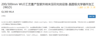
Tenren Nano has Wafer Level Patterning NanoImprint tools, in this case is Wafer Lever Optics and Wafer Lever Stacking, I guess I could be adapted to Wafer Level Packaging.

1732381292086.png
1732381318365.png

Another Good Option will be Direct Write Maskless lithography

CFMEE WLP2000 for Advance Packaging

1732381537054.png


NanoImprint have the issue of defectivity and Direct Write have the issue of throughput.
 
Top