Chinese semiconductor thread II

tokenanalyst

Brigadier
Registered Member

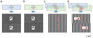
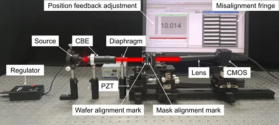
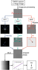
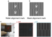
An Improved Algorithm to Extract Moiré Fringe Phase for Wafer-Mask Alignment in Nanoimprint Lithography​

Anhui Province Key Laboratory of Measuring Theory and Precision Instrument, Hefei University of Technology,
Anhui Provincial Engineering Research Center of Semiconductor Inspection Technology and Instrument,
School of Instrument Science and Opto-Electronics Engineering, Hefei University of Technology

Abstract​

This paper proposes an improved algorithm based on the phase extraction of the Moiré fringe for wafer-mask alignment in nanoimprint lithography. The algorithm combines the strengths of the two-dimensional fast Fourier transform (2D-FFT) and two-dimensional window Fourier filtering (2D-WFF) to quickly and accurately extract the fundamental frequencies of interest, eliminate noise in the fundamental frequency band by using the threshold of the local spectrum, and effectively suppress spectral leakage by using a Gaussian window with outstanding sidelobe characteristics while overcoming their limitations, such as avoiding the time-consuming parameter adjustment. The phase extraction accuracy determines the misalignment measurement accuracy, and the alignment accuracy is enhanced to the nanometer level, which is 15.8% and 6.6% higher than 2D-FFT and 2D-WFF, respectively. The results of simulations and experiments confirm the feasibility and rationality of the algorithm.​


1732293537862.png1732293568939.png
1732293664670.png1732293702085.png

Conclusions​

In summary, we propose an improved phase extraction algorithm for wafer-mask alignment in NIL named 2D-FWT. Simulations and experiments verify that our method is more accurate and faster than traditional algorithms (2D-FFT and 2D-WFF). In addition, our algorithm outperforms the existing algorithms in various scenarios, achieving nanometer-level alignment accuracy, which is 15.8% and 6.6% higher than 2D-FFT and 2D-WFF. The 2D-FWT algorithm requires less time for parameter adjustment and is thus suitable for real-time (0.26 s) NIL. With further optimization, this high-precision algorithm can be applied in high-precision measurements based on the fringe phase, such as fringe profilometry, digital holography, and mechanical vibration monitoring.

Please, Log in or Register to view URLs content!
 

tokenanalyst

Brigadier
Registered Member
one more thing, if you read any Chinese article, they mostly write, 28nm and above tools localization are completed but the fact is, we have majority of Non-Litho tools below 28nm completed too like 14nm/7nm and at least shipped to one customer..
Exactly, that is fact that most people are overlooking in that list, every single other tool in that list from the Ion implanters, etching tools to the deposition tools are rated for 28-14/7 nm nanometers.
 

tokenanalyst

Brigadier
Registered Member

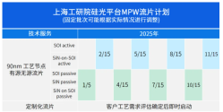
Shanghai Industrial Technology Research Institute 2025 Silicon Photonics MPW tape-out starts​


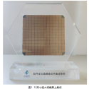
Shanghai Industrial Technology Research Institute (SITRI) has established a silicon-based optoelectronic device process platform in collaboration with well-known domestic research institutions in the field of silicon-based optoelectronics, such as the Shanghai Institute of Microsystem and Information Technology of the Chinese Academy of Sciences, the Institute of Semiconductors of the Chinese Academy of Sciences, and Shanghai Jiao Tong University. It has a clean room of nearly 5,000 square meters and a complete set of key process capabilities, including 90nm high-precision lithography, crystal epitaxy, dielectric thin film growth, dry and wet etching, doping, metal interconnection, and online process detection. It can provide services to various universities, research institutes, and enterprises through MPW, customized tape-out, joint R&D, and other methods to meet customers' diverse needs for R&D, pilot production, and packaging.

1732296066780.png

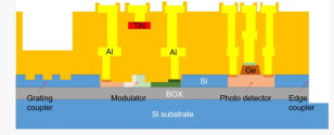
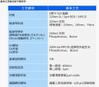
90nm SOI active process

At present, the minimum process node of the 90nm SOI active process tape-out is 90nm . It has key process capabilities such as three-step silicon etching, multi-step active device doping, germanium epitaxy and TiN metal heating electrodes, double-layer aluminum interconnection and deep silicon etching, which can realize various high-performance silicon photonic passive and active devices.

1732296148299.png1732296179612.png

Please, Log in or Register to view URLs content!
 

tokenanalyst

Brigadier
Registered Member

With an investment of 500 million yuan and a monthly output of 5 million kilometers, Yiyuan New Materials' diamond wire project officially went into production.​


Yiyuan New Materials Technology Co., Ltd.'s 5 million kilometers/month diamond wire R&D and production project was held in the Eastern Industrial Park of Yiyang High-tech Zone. It is reported that the total investment of the project is about 500 million yuan .

Yiyang High-tech It is understood that Yujing Co., Ltd. acquired 51% of the equity of Yiyuan New Materials in 2020, and acquired 100% of the equity of Yiyuan New Materials in April 2023. It is a wholly-owned subsidiary of Yujing Co., Ltd. Yiyuan New Materials is a high-tech enterprise focusing on the research, development and production of diamond products and superhard materials. The company's core product is diamond wire, which is widely used in cutting-edge industries such as photovoltaic new energy, magnetic materials , semiconductors, LEDs, etc. With its unremitting pursuit of technological innovation and product quality, Yiyuan New Materials has won many honors such as "Hunan Province's Specialized and New Small and Medium-sized Enterprises", "National High-tech Enterprises", and "Hunan Province New Materials Enterprises". In 2023, the company's diamond wire sales reached 8.76 million kilometers, with an annual output value of 208 million yuan and a tax payment of 6.91 million yuan, making a positive contribution to local economic development.​

Please, Log in or Register to view URLs content!
 

tokenanalyst

Brigadier
Registered Member

Domestic Inductively coupled plasma mass spectrometry for semiconductor manufacturing.​


Inductively coupled plasma mass spectrometry combines inductively coupled plasma (ICP) technology with mass spectrometry (MS) technology. Plasma is used as an ion source. The sample ions ionized in the plasma are introduced into the mass spectrometer through the interface. The mass spectrometer is used to perform mass analysis on the ions (different ions are separated according to the m/Z ratio) and detect and record them.
used in the semiconductor industry.
1. Analysis of impurities on IC silicon wafer surface
2. Photovoltaic polysilicon and monocrystalline silicon impurity analysis
3. Metallic impurities and metal elements in trichlorosilane and silicon tetrachloride.
4. Ultra-pure reagent analysis: ultra-pure inorganic reagents such as hydrofluoric acid, nitric acid, sulfuric acid, hydrochloric acid, ammonia water, hydrogen peroxide, and ultra-pure organic reagents such as isopropyl alcohol (IPA), acetone, tetramethylammonium hydroxide (TMAH), N-methylpyrrolidone (NMP), propylene glycol methyl ether ethyl ester (PGMEA)
5. Ultrapure water analysis
6. High purity gas analysis

1732305820968.png
Please, Log in or Register to view URLs content!

"Analysis of high-purity materials for semiconductors using plasma mass spectrometry"​


Please, Log in or Register to view URLs content!
 

tokenanalyst

Brigadier
Registered Member

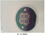
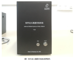
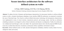
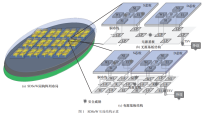
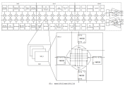
First time seeing this, a Software Defined System of Wafer:

View attachment 139842
Like I said, advanced packaging techniques could surpass traditional IC dimensional scaling in compute and we are talking about serious compute power here.
IC Dimensional Scaling I think could still be dominant on some low power portable applications but in servers, AI, cloud and so on Advanced Packaging will become the dominant technology

1732307959419.png
1732308060582.png1732308113341.png

Please, Log in or Register to view URLs content!
 

tokenanalyst

Brigadier
Registered Member
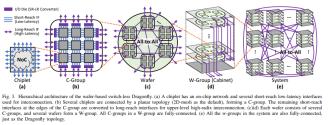
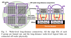
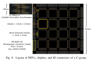
There has been a significant increase in research of Wafer Scale Chips this year.​

Switch-Less Dragonfly on Wafers: A Scalable Interconnection Architecture based on Wafer-Scale Integration​


Institute for Interdisciplinary Information Sciences (IIIS) Tsinghua University, Beijing, China

Abstract:​


Existing high-performance computing (HPC) interconnection architectures are based on high-radix switches, which limits the injection/local performance and introduces latency/energy/cost overhead. The new wafer-scale packaging and high-speed wireline technologies provide high-density, lowlatency, and high-bandwidth connectivity, thus promising to support direct-connected high-radix interconnection architecture. In this paper, we propose a wafer-based interconnection architecture called Switch-Less-Dragonfly-on-Wafers. By utilizing distributed high-bandwidth networks-on-chip-on-wafer, costly high-radix switches of the Dragonfly topology are eliminated while increasing the injection/local throughput and maintaining the global throughput. Based on the proposed architecture, we also introduce baseline and improved deadlock-free minimal/nonminimal routing algorithms with only one additional virtual channel. Extensive evaluations show that the Switch-Less-Dragonflyon-Wafers outperforms the traditional switch-based Dragonfly in both cost and performance. Similar approaches can be applied to other switch-based direct topologies, thus promising to power future large-scale supercomputers.

1732312395559.png
1732312419661.png1732312558868.png

Please, Log in or Register to view URLs content!
 

tokenanalyst

Brigadier
Registered Member

Huadong Heavy Machinery: Ruixin Graphics has achieved mass production and batch supply of GPU chips​


Huadong Heavy Machinery stated on the interactive platform that Ruixin Tuxin has achieved mass production and batch supply of GPU chips.
Thanks to the complete technical adaptation of Ruixin Tuxin in 2023 and the growth of national information and innovation needs in 2024, Ruixin Tuxin has established a cooperative relationship with relevant customers and formed batch supply. At the same time, the company has established a strategic cooperative relationship with Beijing Zhixinwei, a subsidiary of the State Grid, and is jointly committed to the research and development, application and market promotion of independent chips.

In September this year, Huadong Heavy Machinery purchased a total of 37.50% of Ruixin Tuxin's equity (corresponding to a registered capital of 12.62626 million yuan) from Xu Qinghe and Ruifeng Juxin for 74.25 million yuan, and subscribed for Ruixin Tuxin's newly added registered capital of 336,700 yuan for 19.8 million yuan. After the completion of this transaction, the company holds 43.18% of Ruixin Tuxin's equity, making it the single largest shareholder of Ruixin Tuxin.

The announcement shows that Ruixin Tuxin's main business is GPU chips and solutions. Ruixin Tuxin has achieved mass production and batch supply of GPU chips. The current first-generation products are aimed at the domestic localized ICT market. The BF2000 series GPU chips are benchmarked against the main ICT chip products of the domestic leading GPU chip companies. Ruixin Tuxin's GPU has been adapted to domestic mainstream CPUs, operating systems and other ecological manufacturers, and has been used in batches in domestic desktops, all-in-ones, notebooks and tablets. The products have currently entered the party and government office, transportation, education, taxation, electricity and rail transportation industries.

Please, Log in or Register to view URLs content!
 
Top