You are using an out of date browser. It may not display this or other websites correctly.
You should upgrade or use an alternative browser.
You should upgrade or use an alternative browser.
Chinese semiconductor thread II
- Thread starter vincent
- Start date
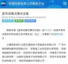
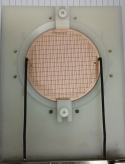
The national standard for direct-write lithography technology led by Xingji Micro-Equipment is officially implemented
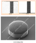
At present, direct-write lithography equipment is widely used and developed in the PCB and pan-semiconductor fields, becoming an emerging micro-nano processing equipment, but there is a lack of national standards for direct-write lithography equipment in the micro-nano processing industry equipment industry. Direct-write lithography technology has significant advantages, such as digital mask design, no need for traditional masks, reducing production costs; simplifying the process flow, greatly shortening the production cycle; improving product yield by reducing process steps; and easy to achieve intelligent management and control, providing strong support for the construction of fully automatic unmanned factories.

In the face of the booming market for direct writing exposure equipment for PCB and IC packaging substrates and the rapid changes in technology, this national standard aims to fill the gap in industry standards and set unified and scientific technical rules for the entire life cycle of equipment, including design, manufacturing, testing, installation and maintenance, quality inspection and assurance, so as to build a complete set of system standards for the industry.
During the standard-setting process, Xingji Micro-Equipment fully utilized its own technical R&D strength and rich practical experience, and actively led and participated in the discussion, research and verification work at all stages, striving to ensure the scientific rationality of the standards, the wide scope of applicability and the foresight of future technological development.
Another major project in Qingdao has been capped, with an estimated annual output value of 3 billion yuan
On September 27, the topping-out ceremony of Qingdao Integrated Circuit Advanced Equipment Park and SIRUI Intelligent Semiconductor Advanced Equipment R&D and Manufacturing Center project was held at Qingdao Integrated Circuit Industrial Park in Qingdao Free Trade Zone and Sino-German Eco-Park.
The Qingdao Integrated Circuit Advanced Equipment Park and SIRUI Intelligent Semiconductor Advanced Equipment R&D and Manufacturing Center project is jointly built by Qingdao Urban Construction Investment (Group) Co., Ltd. and Qingdao Sifang SIRUI Intelligent Technology Co., Ltd. The project covers a total area of about 95 acres and a total construction area of about 86,000 square meters. It plans to build high-end equipment manufacturing production lines such as atomic layer deposition (ALD) and ion implantation (IMP), which will drive social fixed asset investment of about 1.5 billion yuan. It has been selected as a major project of Shandong Province and a key project of Qingdao City in 2024. It is estimated that by 2030, the annual output value of the project will reach 3 billion yuan, creating about 600 jobs.
Li Wei, Party Secretary and Chairman of Qingdao Urban Investment Group, said that as a municipal state-owned capital investment and operation company, Qingdao Urban Investment Group has always taken the initiative to serve the overall situation, the city and the industry, anchored new quality productivity to open up a new development track, and worked with the Free Trade Zone and Sino-German Eco-Park to systematically plan and promote the development of the integrated circuit industry led by chain-leading enterprises, and actively build a development pattern of "building a professional park, introducing a chain-leading enterprise, cultivating an industrial fund, and forming an industrial cluster". Qingdao Urban Investment Group will focus on the rigid needs of chain-leading development and the laws of industrial development, and continue to deepen its layout in Qingdao Integrated Circuit Industrial Park with the innovative model of "urban investment + industrial investment", to help cultivate the industrial ecology and build industrial clusters.
The Institute of Microelectronics has made important progress in GaN device research
Recently, the GaN research team of the High Frequency and High Voltage Center of the Institute of Microelectronics, led by Researcher Liu Xinyu, has conducted innovative research and exploration in research directions such as high-frequency and high-efficiency devices, limiters, and power drive circuits, and has made important progress.
In the field of high-frequency and high-efficiency devices, the team used LP-SiN combined with ALD ultra-thin gate dielectric technology to prepare 0.15μm gate length AlGaN/GaN millimeter-wave MIS-HEMT power devices, which solved the problems of large Schottky leakage and low efficiency of existing HEMT devices. Under continuous wave test conditions, the power added efficiency (PAE) at 30GHz was 49.7% and the power density was 5.90W/mm.
In the direction of limiters, the team used a limiter based on all-GaN SBD-MMIC technology, and used monolithic microwave integrated circuit (all-GaN SBD-MMIC) technology implemented by all-GaN Schottky barrier diodes. The developed limiter showed high incident power of more than 50W in continuous wave mode (CW) and 125W in pulse mode, with insertion loss (IL) less than 1dB@8GHz and a record fast recovery time of 39 nanoseconds, which expanded the application prospects of wide bandgap materials in the field of GaN SBD limiters.
In the direction of power drive circuit, the team developed a GaN-based monolithic envelope tracking power modulator, which integrates the prevention stage required by traditional GaN switching power amplifiers and adopts a double-ended anti-bootstrap circuit to achieve tracking of 20MHz bandwidth and 6.5dB RF envelope signals; the power modulator is used to power the continuous class F PA to realize envelope tracking power amplifier application. At 2.7GHz carrier frequency, 20MHz signal bandwidth, 6.5dB peak-to-average power ratio and 30.6dBm output power, the system efficiency is 8% higher than that of a single PA.
Unisoc's revenue will reach 13 billion yuan, making it the world's tenth largest IC design company!
On September 27, at the third GMIF2024 Innovation Summit, Dr. Liu Zhinong, executive vice president and director of the manufacturing business department of domestic chip giant Unisoc, revealed that although the global smartphone market shipments in 2023 fell by 3.2% year-on-year, Unisoc's revenue still exceeded 13 billion yuan.
well, if China really wanted to. Infineon wouldn't be producing any GaN chips.Propaganda about how Infineon was supposedly the first company to produce 300mm GaN wafers for power applications.
Reality. A Chinese company already did that three years ago.
I did a semi-deep dive into China and Gallium yesterday and the control that China has over Gallium is basically unshakeable at this point.
Guanghua Technology's wafer-level cyanide-free gold plating industrialization promotes the localization of semiconductor laser device manufacturing
In the fierce international competition in the semiconductor industry, Chinese companies are gradually emerging. Recently, Guanghua Technology has made a major breakthrough in wafer-level cyanide-free gold plating technology, which has been successfully applied to semiconductor laser devices and achieved mass production in semiconductor wafer manufacturing. This milestone breakthrough marks another major progress in China's domestic substitution process in the semiconductor field. As a leader in electroplating technology, Guanghua Technology has injected strong impetus into the independent control of the semiconductor industry supply chain with its leading cyanide-free gold plating liquid products and technologies.


Annual output of 30,000 tons! Guangdong Meizhou high-purity quartz sand project held a production ceremony
The 30,000-ton high-purity quartz sand automated production line project was invested and built by Pingyuan Shuangmu New Materials Co., Ltd. In June this year, the Pingyuan Branch of the Meizhou Ecological Environment Bureau planned to approve the environmental impact assessment document of the Shuangmu 30,000-ton high-purity quartz sand and 5,000-ton quartz flange automated production line construction project. The document shows that Pingyuan Shuangmu New Materials Technology Co., Ltd. plans to rent a factory in Guangzhou Nansha (Pingyuan) Industrial Transfer Industrial Park to invest in the construction of the "Shuangmu 30,000-ton high-purity quartz sand and 5,000-ton quartz flange automated production line construction project". The project aims to design and build a comprehensive quartz product production line, mainly covering the production of high-purity quartz sand and quartz flanges. The overall production capacity is planned to produce 30,000 tons of high-purity quartz sand and 5,000 tons of quartz flanges per year. The project is divided into two phases. The first phase includes an annual production line of 15,000 tons of high-purity quartz sand and an annual production line of 5,000 tons of quartz flanges. The second phase is an annual production line of 15,000 tons of high-purity quartz sand. Of the 30,000 tons of high-purity quartz sand produced annually by this project, 21,000 tons will be sold directly as products to meet market demand, and the remaining 9,000 tons will be used for deep processing to produce quartz flanges to fully utilize resources and increase product added value.
One is on SiC and other is on Si.Propaganda about how Infineon was supposedly the first company to produce 300mm GaN wafers for power applications.
Reality. A Chinese company already did that three years ago.
