Chinese semiconductor thread II

Blitzo

Lieutenant General
Staff member
Super Moderator
Registered Member
So what difference will all of this new companies/institutions make? If they are so good, why didn't they go help out SMEE in their development 10 years ago, or 6 years ago when the sanctions made the threat of even basic DUV machines being cut of very real?

Because decades ago, 10 years ago (and even 6 years ago), there was limited impetus to seriously drive for domestic products, given they could attain foreign products that were more competitive and available through trade and the "free market".

The lack of demand and need meant that government strategic directives alone would not be enough to force customers to take a risk on products that were less capable and less mature than established overseas players, all while still trying to attain a profit and compete with foreign companies as well as other domestic companies.

But it is only in the last few years that the customers in China truly realized how vulnerable they were to sanctions and being cut off, which has resulted in the emerging captive market that we are starting to see and the entire tech stack re-orientate.


If your question is why has it taken SMEE so long to develop domestic DUV that customers would find viable, I would actually flip the question around and ask why do we think it could have been done faster? Where was the need, the demand or the urgency for domestic DUV machines until the last few years?
Even if we want to talk about DUVs, the fact that customers have been able to buy ASML DUVs in the last couple of years has likely produced a slight drag effect on the priority and urgency of SMEE's DUV product.
 

european_guy

Junior Member
Registered Member
The only way I can see of stopping China from creating not only a mere EUV and DUV immersion lithography machine but an entire EUV and DUVi lithography supply chain that includes the mass production of wafers-reticle stages, DUV and EUV optics and mirrors, ultrapure water systems, EUV and DUV light sources, advanced positioning sensors, lithography machines parts and components, overlay metrology machines, OPC software, CDSEM and others ADI and AEI machines, EUV-DUVi photoresist, DUVi and EUV mask manufacturing and so on and on, is:

If ASML sells then their EUV and DUVi machines with not restrictions or a nuclear war, beyond that I don't see any way.

I'd really hope for the first :)

The ongoing discussion regarding EUV / DUV IMHO misses a key point: the totally different expected market size.

In China only SMIC and maybe later CXMT will use EUV, with YMTC eventually joining the group much later (like 4/5 years later), and nobody will ever buy a Chinese EUV machine outside China (for many reasons).

Instead DUV Arf/Krf/i-line litho machines of SMEE will be the bread and butter of China semi industry because they will have to replace ASML/Japan machines in the medium/long term. And potentially they will eventually also be sold outside China.

So this difference yields to 2 totally different approaches.

For DUV machines you want a standard company that designs, manufactures and sells their products in volume production and can compete with ASML/Japan on performance/cost and (last but not least) returns a profit at the end of the year. IOW a healthy company.

Instead for EUV the research institute / state academy approach makes perfectly sense: numbers will be forever low, EUV machines will be a limited sequence of "single units", investment will be huge, ROI non existent. From financial/business POW this is the approach you take when you want to send a space station to the moon! Single samples, very expensive, with a lot of advanced R&D, but at loss by design, with the foreseen return given in broader terms of improving national tech level and self-sufficiency.

I'm not surprised EUV is developed by state research institutes, differently from ASML, hardly there will be a world market for China EUV machines, and for a private company it would not hold the business case.
 
Last edited:

tphuang

Lieutenant General
Staff member
Super Moderator
VIP Professional
Registered Member
I'd really hope for the first :)

The ongoing discussion regarding EUV / DUV IMHO misses a key point: the totally different expected market size.

In China only SMIC and maybe later CXMT will use EUV, with YMTC eventually joining the group much later (like 4/5 years later), and nobody will ever buy a Chinese EUV machine outside China (for a lot of reasons).

Instead DUV Arf/Krf/i-line litho machines of SMEE will be the bread and butter of China semi industry because they will have to replace ASML/Japan machines in the medium/long term. And potentially they will eventually also sold outside China.

So this difference yields to 2 totally different approaches.

For DUV machines you want a standard company that designs, manufactures and sells their products in volume production and can compete with ASML/Japan on performance/cost and (last but not least) returns a profit at the end of the year. IOW an healthy company.

Instead for EUV the research institute / state academy approach makes perfectly sense: numbers will be forever low, EUV machines will be a limited sequence of "single units", investment will be huge, ROI non existent. From financial/business POW this is the approach you take when you want to send a space station to the moon! Single samples, very expensive, with a lot of advanced R&D, but at loss by design, with the foreseen return given in broader terms of improving national tech level and self-sufficiency.

I'm not surprised EUV is developed by state research institutes, differently from ASML, there will never be a world market for China EUV machines, and a private company would not hold the business case.
you forgot Huawei. They will want the EUV for sure. They will try cutting edge logic and DRAM production
 

PopularScience

Junior Member
Registered Member
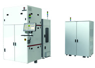
Said to be pair with SSX800

Please, Log in or Register to view URLs content!

SHM800 Holistic Metrology Equipment

SHM800.jpg

SHM800

SHM800 holistic metrology equipment is an optical scatterometry-based system. SHM800 is mainly used in advanced process (55nm~7nm). It can offer the high precision overlay measurement, and has a throughput to match the productivity of lithography scanner. Working with the process control, SHM800 can improve the performance of scanner in overlay error control.
u177.png
Product Features
Match the requirement of Logic, Memory, Dram and other advanced technology in overlay measurement.

High-speed measurement for a large number of sampling.

Compatible with micro-marking to meet advanced node In-die measurement.

Provide multi-dimensional adjustable configuration for different process layer stacks.

Provide automatic tools to optimize the measurement configuration.

Holistic lithography solutions to improve overlay performance.
 

european_guy

Junior Member
Registered Member
you forgot Huawei. They will want the EUV for sure. They will try cutting edge logic and DRAM production

If we are talking of 10 years from now, anything can happen. But in this decade Huawei has (still) no experience running a fab, even less an advanced one.

A couple of years ago they tried to poach engineers from SMEE to build their litho machine, it ended up in a big no-no (with gov. intervention, and they did the right call IMHO), if they now poach from SMIC (the only way to ramp up an advanced fab in a relatively short time) it would be another no-no....at least for the foreseeable future.

As like with SMEE case (where 130 Huawei engineers eventually joined the SMEE's R&D), we can foresee that eventually Huawei guys will help SMIC to setup a couple of lines for Huawei, eventually with exclusivity of use grant, but always inside SMIC....this option seems far more realistic.

@sunnymaxi please consider that the business case for EUV is still far from being decided, even years later. The new high NA machine from ASML has at best
Please, Log in or Register to view URLs content!
, and this is supposed to be the future....
 
Last edited:

sunnymaxi

Captain
Registered Member
you forgot Huawei. They will want the EUV for sure. They will try cutting edge logic and DRAM production
i would say, SMIC itself has enormous demand for EUV in regards with world's factory. if they really want to become world largest fab company like TSMC. lets suppose all Chinese customers switch to SMIC.

so Huawei+SMIC and CXMT are surely EUV customers. maybe some other companies join this list if EUV is available.

@european_guy agreed with your post except EUV demand in mainland..
 

tphuang

Lieutenant General
Staff member
Super Moderator
VIP Professional
Registered Member
If we are talking of 10 years from now, anything can happen. But in this decade Huawei has (still) no experience running a fab, even less an advanced one.

A couple of years ago they tried to poach engineers from SMEE to build their litho machine, it ended up in a big no-no (with gov. intervention, and they did the right call IMHO), if they now poach from SMIC (the only way to ramp up an advanced fab in a relatively short time) it would be another no-no....at least for the foreseeable future.

As like with SMEE case (where 130 Huawei engineers eventually joined the SMEE's R&D), we can foresee that eventually Huawei guys will help SMIC to setup a couple of lines for Huawei, eventually with exclusivity of use grant, but always inside SMIC....this option seems far more realistic.
do you know that Swaysure bought a few NXT2050i?

It's a mistake to underestimate Huawei's ambition even in near term
 

ZeEa5KPul

Colonel
Registered Member
I find it helpful to occasionally summarize what we "know" about China's EUV effort. Additions/corrections from knowledgeable members welcome.

Light Source​

There are three EUV light source projects being investigated in China: CIOMP's LPP (laser pulse plasma), Tsinghua University's SSMB (steady state microbunching) at Xiong'an New Area, and Shenzhen's FEL (free electron laser).

SSMB: This seems to be the most promising long term solution to commercial EUV light sources and success here would allow China to leapfrog market leaders. However, what I gathered from reading research papers about this is that the challenges are significant. SSMB is still in very early stages with a synchrotron being built in Xiong'an New Area, so it's certain not to be part of China's first EUVL device.

LPP: This has the benefit of an existing proof of principle. We hear rumours that this component is part of an assembled 500W prototype EUV scanner, but things are understandably shrouded in secrecy. This is the most developed of the approaches China is trying and is likely to be first to market. Even here China is experimenting with several laser mechanisms. CIOMP's prototype uses a CO2 MOPA laser, following the approach taken by ASML. There have been some papers published examining the use of fiber lasers in a LPP device, but this is not the approach CIOMP is taking, at least not with the first machine.

FEL: I know very little about this work and I'm skeptical of its viability. FEL was one of the approaches initially investigated for EUV light generation in lithography and rejected because the output is not continuous enough. FELs take too long to recharge between each "shot." In fact, SSMBs were developed to get around this limitation of FELs, and SSMB can be thought of as a hybrid between a FEL and a synchrotron.

Optics​

EUV utilizes purely reflective optics (curved mirrors). Refraction is impossible since EUV light is absorbed by nearly every medium (air, water, silica, etc.) These mirrors are constructed from alternating layers of silicon and molybdenum, each a few nanometers thick and up to 80 layers per mirror.

A good proxy for how China is able to manufacture these mirrors is to examine how proficient it is at the core competencies of advanced industry: high-quality vacuums, precise temperature control, atomic deposition processes like PVD, grinding and polishing curved surfaces, very accurate metrology to measure the thickness and roughness of layers.

These are all broadly applicable throughout advanced industry. For example, vacuums and maintaining precise temperature gradients are critical for the preparation and casting of nickel alloys to produce gas turbines. Grinding, polishing, and accurate metrology are crucial to preparing satellite optics. In fact, CIOMP itself has created a 4m diameter silicon carbide mirror speculated to be the primary sensor aboard the Yaogan-41 satellite:

Please, Log in or Register to view URLs content!

Wafer Stage​

The Harbin Institute of Technology is rumoured to be the provider of CIOMP's prototype's wafer stage, and it has a lot of core competencies in this field:

Please, Log in or Register to view URLs content!

Harbin is supplying interferometers to both the EUV and DUV efforts. Indeed, positioning accuracy is one of, if not the, most important factors in determining multipatterning accuracy, which itself is the primary determinant of how far a DUVi process can be pushed from 28nm down to 5nm.
 

tokenanalyst

Brigadier
Registered Member
I'd really hope for the first :)

The ongoing discussion regarding EUV / DUV IMHO misses a key point: the totally different expected market size.

In China only SMIC and maybe later CXMT will use EUV, with YMTC eventually joining the group much later (like 4/5 years later), and nobody will ever buy a Chinese EUV machine outside China (for many reasons).

Instead DUV Arf/Krf/i-line litho machines of SMEE will be the bread and butter of China semi industry because they will have to replace ASML/Japan machines in the medium/long term. And potentially they will eventually also be sold outside China.

So this difference yields to 2 totally different approaches.

For DUV machines you want a standard company that designs, manufactures and sells their products in volume production and can compete with ASML/Japan on performance/cost and (last but not least) returns a profit at the end of the year. IOW a healthy company.

Instead for EUV the research institute / state academy approach makes perfectly sense: numbers will be forever low, EUV machines will be a limited sequence of "single units", investment will be huge, ROI non existent. From financial/business POW this is the approach you take when you want to send a space station to the moon! Single samples, very expensive, with a lot of advanced R&D, but at loss by design, with the foreseen return given in broader terms of improving national tech level and self-sufficiency.

I'm not surprised EUV is developed by state research institutes, differently from ASML, hardly there will be a world market for China EUV machines, and for a private company it would not hold the business case.
The machines of the EUV project are already sold in China for the companies working in this project, Huawei, SMIC, YMTC and probably HHGrace and CXMT. You maybe right that "maybe" there will not be a market for Chinese EUV machine outside China but like a I said before is NOT just a mere lithography machine but an entire supply chain. What about EUV photoresist, or future EUV inspection machines, EUV light sources like the DPP that I posted before, multilayer coating system, the high vacuum technologies of this project, EUV mask services, EUV related materials, future Kingsemi EUV coating and developing systems, etc. And in world were companies a looking to reduce cost and increase profits is logical to think that a lot of that is going to make it outside.

If you do the research deep enough your will found out that a lot of Chinese companies are postioning themselves to take a chunk of the near future Chinese EUV market.
 

FairAndUnbiased

Brigadier
Registered Member
Said to be pair with SSX800

Please, Log in or Register to view URLs content!

SHM800 Holistic Metrology Equipment

SHM800.jpg

SHM800

SHM800 holistic metrology equipment is an optical scatterometry-based system. SHM800 is mainly used in advanced process (55nm~7nm). It can offer the high precision overlay measurement, and has a throughput to match the productivity of lithography scanner. Working with the process control, SHM800 can improve the performance of scanner in overlay error control.
u177.png
Product Features
Match the requirement of Logic, Memory, Dram and other advanced technology in overlay measurement.

High-speed measurement for a large number of sampling.

Compatible with micro-marking to meet advanced node In-die measurement.

Provide multi-dimensional adjustable configuration for different process layer stacks.

Provide automatic tools to optimize the measurement configuration.

Holistic lithography solutions to improve overlay performance.
Holy shit. This is top-tier optical metrology equipment.
 
Top