Chinese semiconductor thread II

tokenanalyst

Brigadier
Registered Member

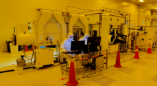
Jihua Laboratory has made a major breakthrough in the research of high-resolution OLED inkjet printing equipment​


Compared with traditional OLED panel evaporation technology, OLED inkjet printing technology has on-demand printing and high material utilization (evaporation process material utilization rate is <15%, inkjet printing can increase to more than 85%), and does not require high With the advantages of precision mask and no need for vacuum environment, it is the most potential luminescent layer forming method for making large-size OLED panels. It is becoming a major technological revolution in the new display industry and is also hailed as completely changing the current OLED electronic display industry. A disruptive industrial technological revolution that transforms "evaporation process" into "inkjet printing" technology.
1707171967546.png

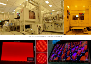
Professor Zhu Yunlong’s team in Jihua Laboratory has been committed to developing high-resolution OLED inkjet printing equipment. The team spent more than 3 years and successively achieved breakthroughs in macro-volume inkjet printing synchronous collaborative control technology, large-scale cavity multi-physics and high stability It has formed a unique inkjet printing technology solution using a number of key core technologies such as sex controllable technology, high-precision alignment system, and high-precision circulating ink supply system. It has successfully developed a complete set of 200mm×200mm OLED inkjet printing equipment and achieved 7 The full-color printing and lighting of 137-inch 137ppi substrates, the printing and UV testing of 5-inch 254ppi and 300ppi substrates mark the first time that my country's independent equipment has achieved high-resolution printing of 300ppi, and its performance has reached the international advanced level.
1707171991324.png

Please, Log in or Register to view URLs content!
 

tokenanalyst

Brigadier
Registered Member
More local components manufacturers. High end valves for the semiconductor industry.

Ningbo Instrument Valve Factory​


Vacuum valves are widely used in the semiconductor industry and can be said to be one of the key equipment in the semiconductor manufacturing industry. Their main function is to control and regulate gas flow, maintain a vacuum environment, and ensure stability and reliability in the semiconductor production process.

The semiconductor industry mainly includes the following categories:

1. Chip manufacturing: involves chip design, chip packaging, chip testing, etc.
2. Component manufacturing: involves the production of semiconductor devices (transistors, integrated circuits, optoelectronic components, etc.).
3. Integrated circuit design: design involving hardware, software, simulation, mixed signal and other fields.
4. System integration: involves the assembly and testing of semiconductor components, circuits, software, and systems.
5. Semiconductor equipment manufacturing: involves the manufacturing and maintenance of semiconductor equipment.
6. Semiconductor chip applications: involve the application of semiconductor chips in fields such as computers, consumer electronics, and communication.


The vacuum system has strict requirements for vacuum valves
The vacuum system includes various components, such as chambers, pumps, valves, etc., which have strict parameter requirements and high research and production difficulties. Only in material selection, many factors need to be considered in combination with application, environmental conditions, and the degree of vacuum to be achieved. And it also requires complex and precise welding, surface treatment, cleaning and other processes, among which the vacuum valves required are best selected from manufacturers who have accumulated professional vacuum technology in the industry for a long time.

Specifically, in terms of vacuum valve products, excellent sealing performance, precise flow control, minimal particle generation, minimal vibration and impact, stability and repeatability are also crucial characteristics. Especially in semiconductor manufacturing, which has extremely high requirements for purity, chemical and physical stability of the process environment, its requirements will be higher than standard vacuum valves.

Choosing a professional manufacturer for semiconductor vacuum valves
Ningbo Instrument Valve Factory has been focusing on research in the field of vacuum technology since its establishment in 1964. Its torch brand is a well-known brand in the vacuum industry, and its vacuum valve products such as vacuum plug valves, vacuum baffle valves, vacuum ball valves, and vacuum butterfly valves have mature processes and are well-known overseas. They can be applied to different types of vacuum equipment in the semiconductor industry, and the valves are driven by manual, pneumatic, and electric devices, To achieve precise control and regulation of gas flow rate and flow rate, with better sealing and regulation performance.

Please, Log in or Register to view URLs content!
 

FairAndUnbiased

Brigadier
Registered Member
Please, Log in or Register to view URLs content!

I am not sure how seriously to take this. If Samsung initial attempt at gaafet is this bad, then we may be further out from gaafet hvm than a lot of people thought.
as I expected based on previous trends of per wafer costs by process (which is related to both process difficulty and yield, as bad wafers have to be subsidized by good wafers) there are likely to be very few applications for 3 nm GAAFET compared to advanced packaging + 7 nm.
 

latenlazy

Brigadier
as I expected based on previous trends of per wafer costs by process (which is related to both process difficulty and yield, as bad wafers have to be subsidized by good wafers) there are likely to be very few applications for 3 nm GAAFET compared to advanced packaging + 7 nm.
Honestly given that TSMC also struggled with 3 nm on a FinFET architecture I'm beginning to wonder if the shrinking game is still tenable as a driver for performance. Makes me wonder if it wouldn't be a better strategy to stay at a larger node and focus innovation on transistor architecture.
 

gelgoog

Lieutenant General
Registered Member
Having 0% yields does not mean anything without having the proper context. Assuming it is even true.

But yeah it sounds bad. And it is not that unexpected really. Samsung's GAAFET process is supposedly based on IBM's. And IBM was never well known for having good yields in any of their processes. IBM always focused on performance vs manufacturability while Samsung used to be the other way around before they allied with IBM and Globalfoundries in process development. Now that IBM mostly use other people's fabs and only do R&D it is probably even worse.

Samsung is basically betting the farm on a new transistor architecture to try to steal market share from TSMC. It was a risky bet, and it might fail.
TSMC tried to mitigate these risks by continuing to use FinFET for 3nm.
 
Last edited:

latenlazy

Brigadier
Having 0% yields does not mean anything without having the proper context. Assuming it is even true.

But yeah it sounds bad. And it is not that unexpected really. Samsung's GAAFET process is supposedly based on IBM's. And IBM was never well known for having good yields in any of their processes. IBM always focused on performance vs manufacturability while Samsung used to be the other way around before they allied with IBM and Globalfoundries in process development. Now that IBM mostly use other people's fabs and only do R&D it is probably even worse.

Samsung is basically betting the farm on a new transistor architecture to try to steal market share from TSMC. It was a risky bet, and it might fail.
TSMC tried to mitigate these risks by continuing to use FinFET for 3nm.
I don't really believe the 0% yield at face value. But I think we have a lot of evidence over the last 3 years that 3 nm is a lot harder than either TSMC or Samsung were hoping, and GAA is such a complex nanoscale architecture to try to get good quality control on.
 

LanceD23

New Member
Registered Member
whos supplying photoresist to SMIC production as Japan banning supplying chemicals and equipments for anything below 45nm? japan controls 70% of that market.
 

tokenanalyst

Brigadier
Registered Member
as I expected based on previous trends of per wafer costs by process (which is related to both process difficulty and yield, as bad wafers have to be subsidized by good wafers) there are likely to be very few applications for 3 nm GAAFET compared to advanced packaging + 7 nm.
For I have been reading looks like the problem could be a problem of patterning the memory cells inside their processors, last time I remember they were getting decent yields making mining chips but then again those are more simpler chips than SoCs.
 

tphuang

Lieutenant General
Staff member
Super Moderator
VIP Professional
Registered Member
i'm also not a believer of 0%, but I think it's clear that GAAFET is a big jump from FinFet.

Getting acceptable yield in HVM for something like phone SoC is probably going to take longer than usual.

Took 3 years basically to go from mass produced A14 to A17. Will TSMC get N2/GAA ready for HVM with acceptable yield for A19 or A20 or A21? I'd have a hard time believing it will get to that place with A19
 
Top