Chinese semiconductor thread II

tokenanalyst

Brigadier
Registered Member

Paixin Semiconductor Packaging and Testing Equipment Headquarters Project Signed with Suzhou High-tech Zone​

The Paixin Semiconductor Packaging and Testing Equipment Headquarters Project was signed and landed in Suzhou High-tech Zone.

According to news released by Suzhou High-tech Zone, Suzhou Paixin Semiconductor Technology Co., Ltd. focuses on the research and development, manufacturing and sales of advanced chip packaging and testing equipment. Its main products include advanced packaging flip-chip equipment, advanced placement machines, mass testing machines and third-party testing machines. Third generation semiconductor wafer inspection equipment, etc. The newly launched Paixin Semiconductor Packaging and Testing Equipment Headquarters will introduce advanced technology and production lines to create a company headquarters integrating production and research and development.

In recent years, the integrated circuit industry in Suzhou High-tech Zone has developed rapidly. It has institute platforms such as the East China Branch of the Fifth Electronics Institute of the Ministry of Industry and Information Technology, the national-level Suzhou Semiconductor Laser Innovation Center, and the Jiangsu Provincial Board Integrated Circuit and Component Adaptation Verification Center. The scale of the industry continues to grow, with more than 250 related companies such as Guoxin Technology gathered together, and a total of 8 listed companies have been cultivated, with the industry scale exceeding 22 billion yuan. The industrial ecology has been continuously optimized. An industrial fund of funds with a total scale of 10 billion yuan and a science and technology angel fund with a total scale of 2 billion yuan have been established. It has more than 2 million square meters of specialized carriers such as the Suzhou Integrated Circuit Innovation Center.

Please, Log in or Register to view URLs content!
 

tokenanalyst

Brigadier
Registered Member

The first WLP2000 for Bumping in the Year of the Dragon is shipped to advanced packaging head customers​


Xinqi Micropackaging is a provider of direct-write lithography solutions for the advanced packaging market. The continuous and repeated delivery of WLP2000 wafer-level advanced packaging direct-write lithography equipment orders is changing the advanced packaging industry.

1706969983563.png


The WLP2000 direct-write lithography equipment meets the requirements of the semiconductor industry with flexible digital masks and high yield rates. This equipment can solve the offset interconnection problem between chips due to the positioning error of the placement equipment during the combination of multiple chips through intelligent rewiring RDL technology based on the measurement results of the position of each Die; real-time automatic focusing The module can compensate for substrate warpage or topographic deformation; advanced digital mask technology can handle the problem of low efficiency caused by continuous exposure pattern splicing when packaging large-size wafer-level chips; and various types of additions can be added to each exposure Industrial barcode and other patterns.

The WLP2000 direct-write lithography equipment has significant advantages such as high resolution, high productivity, and full automation. It can be seamlessly integrated into customer production lines and achieve mass production with resolutions as low as 2 μm. Customers do not need to perform mask management, which reduces production costs, shortens time cycles and reduces workload. The modular design enables fast maintenance and after-sales, longer life of the laser and less energy and consumables, reducing the customer's TCO.

This equipment delivery is a continuous repeat order from China's leading advanced packaging customer, and the stability and functionality of the product have been verified. The WLP2000 direct-write lithography equipment was launched on the market at the end of 2019. It is the first direct-write lithography equipment in China specifically designed for mass production applications of advanced wafer-level packaging.​

Please, Log in or Register to view URLs content!
 

tokenanalyst

Brigadier
Registered Member

Xinhe Semiconductor releases SI/PI/multiphysics analysis EDA solution at DesignCon2024 conference.​


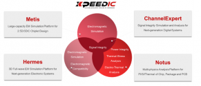
Xinhe Semiconductor officially released the SI/PI/multiphysics analysis EDA solution for next-generation electronic systems at the just-concluded DesignCon 2024 conference , including signal integrity, power integrity, Multiple EDA analysis platforms such as electromagnetic simulation, thermal and stress.

  • Please, Log in or Register to view URLs content!
    has rich pre-wiring simulation analysis functions and integrates the Interposer template of the industry's mainstream 2.5D/3D process technology. Users can customize the wiring form and set parameters to complete Interposer wiring efficiently and accurately.
  • Please, Log in or Register to view URLs content!
    provides three major electromagnetic simulation analysis tools, Hermes Layered, Hermes 3D and Hermes X3D, for packaging/PCB board-level systems and other subdivided application scenarios, which respectively meet the needs of packaging and board-level signal model extraction, and arbitrary three-dimensional structures.
  • Please, Log in or Register to view URLs content!
    Based on Xinhe Semiconductor's powerful electromagnetic field and multi-physics simulation engine technology, it provides users with a more efficient and automatic way to meet design needs in signal integrity, power integrity, thermal and stress analysis.
  • Please, Log in or Register to view URLs content!
    , the next generation digital system signal integrity simulation analysis platform, is based on graphical circuit simulation interaction and provides users with a fast, accurate and simple method to analyze high-speed channels. ChannelExpert has a complete set of high-speed channel comprehensive analysis functions, including frequency domain S parameters, time domain eye diagrams, statistical eye diagrams, COM, and parametric scanning and optimization.
1706975494504.png

Please, Log in or Register to view URLs content!
 

tokenanalyst

Brigadier
Registered Member

Jingxu Semiconductor received a strategic investment of 100 million yuan to promote the completion of an annual production of 750,000 gallium oxide epitaxial wafers.​


Shenzhen Ruiyue Investment Holding Group Co., Ltd. (hereinafter referred to as "Ruiyue Holding Group") and Fujian Jingxu Semiconductor Technology Co., Ltd. (hereinafter referred to as "Jingxu Semiconductor") signed a strategic investment The ceremony is held.

As the exclusive strategic investor of Jingxu Semiconductor, Ruiyue Investment has strategically invested RMB 100 million in Jingxu Semiconductor to help achieve the annual production capacity of 750,000 gallium oxide epitaxial wafers and 1.2 billion filter chips.

Please, Log in or Register to view URLs content!


tphuang

Lieutenant General
Staff member
Super Moderator
VIP Professional
Registered Member

Jingxu Semiconductor received a strategic investment of 100 million yuan to promote the completion of an annual production of 750,000 gallium oxide epitaxial wafers.​


Shenzhen Ruiyue Investment Holding Group Co., Ltd. (hereinafter referred to as "Ruiyue Holding Group") and Fujian Jingxu Semiconductor Technology Co., Ltd. (hereinafter referred to as "Jingxu Semiconductor") signed a strategic investment The ceremony is held.

As the exclusive strategic investor of Jingxu Semiconductor, Ruiyue Investment has strategically invested RMB 100 million in Jingxu Semiconductor to help achieve the annual production capacity of 750,000 gallium oxide epitaxial wafers and 1.2 billion filter chips.

Please, Log in or Register to view URLs content!

wow, this is crazy. Gallium oxide RF BAW filters? I've never heard of this before. going to have to read up on this.
 

tphuang

Lieutenant General
Staff member
Super Moderator
VIP Professional
Registered Member
Looks like they were found in Nov 2020
Please, Log in or Register to view URLs content!

Won award in February for their gallium oxide piezoelectric thin film material BAW filter. It's the first company in the world to mass produce Ga23 based BAW filter

Please, Log in or Register to view URLs content!

Looks like they are just producing 2-inch wafers right now. So that's probably why their annual production is 750k. Those are really small wafers
Please, Log in or Register to view URLs content!

I'm still waiting of the diamond BAW filter news to get updated
 

caudaceus

Senior Member
Registered Member
Looks like they were found in Nov 2020
Please, Log in or Register to view URLs content!

Won award in February for their gallium oxide piezoelectric thin film material BAW filter. It's the first company in the world to mass produce Ga23 based BAW filter

Please, Log in or Register to view URLs content!

Looks like they are just producing 2-inch wafers right now. So that's probably why their annual production is 750k. Those are really small wafers
Please, Log in or Register to view URLs content!

I'm still waiting of the diamond BAW filter news to get updated
Huaqiangbei selling radar modules better than anything Raytheon can source is not in my Bingo card
 

european_guy

Junior Member
Registered Member
SMIC Q4 financials results next week

Wednesday 7 there will be SMIC Q4's results conference call

Please, Log in or Register to view URLs content!

Very important event, hopefully we will have some hint (I don't expect full disclosure) to advanced node's current capacity. It should be anywhere between 15K and 25K wpm, according to knowledgeable people in this forum.

My impression is that Huawei is pushing them really hard. Not only chips for mobile phones and AI, but now also critical components for ADAS seems to be in delay

Please, Log in or Register to view URLs content!

MDC 810, or Mobile Digital Computation, runs on a standard platform-based format. It can achieve the high-stream computing power of 400 TOPS

This seems to be and AI chip for autonomous driving, almost surely manufactured by SMIC (400 tops requires advanced node).

Huawei in a somewhat euphoric reaction after gaining access again to advanced foundry services after many years IMHO is going in overdrive mode: mobile phones, AI for data centers, ADAS chips for cars and maybe there will be even more....the poor guys at SMIC have to work h24 7/7 to satisfy at least partially Huawei insatiable appetite for advanced chips.

Urgent increase of capacity / yields has never been so important for SMIC, no matter how expensive.
 
Last edited:

FairAndUnbiased

Brigadier
Registered Member
Looks like they were found in Nov 2020
Please, Log in or Register to view URLs content!

Won award in February for their gallium oxide piezoelectric thin film material BAW filter. It's the first company in the world to mass produce Ga23 based BAW filter

Please, Log in or Register to view URLs content!

Looks like they are just producing 2-inch wafers right now. So that's probably why their annual production is 750k. Those are really small wafers
Please, Log in or Register to view URLs content!

I'm still waiting of the diamond BAW filter news to get updated
50 mm wafer is common for prototype MEMS/sensor products.

AMEC already has an 18x batch system for 50 mm MOCVD.

Please, Log in or Register to view URLs content!
 

tphuang

Lieutenant General
Staff member
Super Moderator
VIP Professional
Registered Member
50 mm wafer is common for prototype MEMS/sensor products.

AMEC already has an 18x batch system for 50 mm MOCVD.

Please, Log in or Register to view URLs content!
that's fine. I'm not expecting them to go beyond that. After all, they only got 6/8-inch wafers grown a year ago, commercialization will take a while.

Getting yield up in 2-inch production is the key. This is brand new tech after all.
 
Top