Chinese semiconductor thread II

tokenanalyst

Brigadier
Registered Member

Navigating export controls​

Dutch chips manufacturer ASML, one of Europe’s biggest companies in this sector, is the latest business to feel the impact. Last week it
Please, Log in or Register to view URLs content!
to China of two types of deep ultraviolet lithography machines – key components in chipmaking – because its export licence was “partially revoked by the Dutch government.”

The UK government, meanwhile,
Please, Log in or Register to view URLs content!
for British companies seeking to export semiconductor technology to China in 2023, and approved just two, according to official data. That represents a refusal rate of 87.5%; in 2022 it rejected just 16% of applications.

Startup founders have got the message; some of them are deciding against selling their machines to China to avoid the bureaucratic hassle of a rejected export application.

Simon Thomas, founder and CEO of Paragraf, a Cambridge-based startup developing graphene-based semiconductors, says his company decided not to sell a magnetic field sensor, capable of operating in high-radiation environments, in China because it could have been of interest to the Chinese military.

Paragraf is close to commercialising other biosensors — tiny smart devices based on semiconductors which are replacing costly conventional sensors across many applications including navigation systems and health monitors — and Thomas says these are more likely to be subject to UK government export restrictions.
I do really hope the China don't impose too much exports controls to Western countries because I would absolutely love to see China flooding the European and US market with the same technologies that Western companies are not allow to sell inside China, It will be hilarious seeing US companies competing against Chinese companies with their hands tie in the back by their goverment.
It remembers me when the US decided to civilian drones into ITAR list while DJI was selling their phantom drones everywhere, guess who took over the drone market.


ansy1968

Brigadier
Registered Member
I have translated it and wondering whether it is only for 2023 delivery and what month status? wondering how many total 2050i machines SMIC has as at the end of 2023?

I am expecting a bit more than 2 units SMEE SSA/800 in 2023 delivery .... @ansy1968 any news or rumours you have heard? hopefully SSA/900 can be delivered in 2024 for testing

Interesting that Nikon still selling immersion scanner Nikon 635

View attachment 123595
Sir, I'm holding this news report for 5 months now, I want to authenticated it first before posting, due to busy schedule I nearly forget to post it until I see your post.

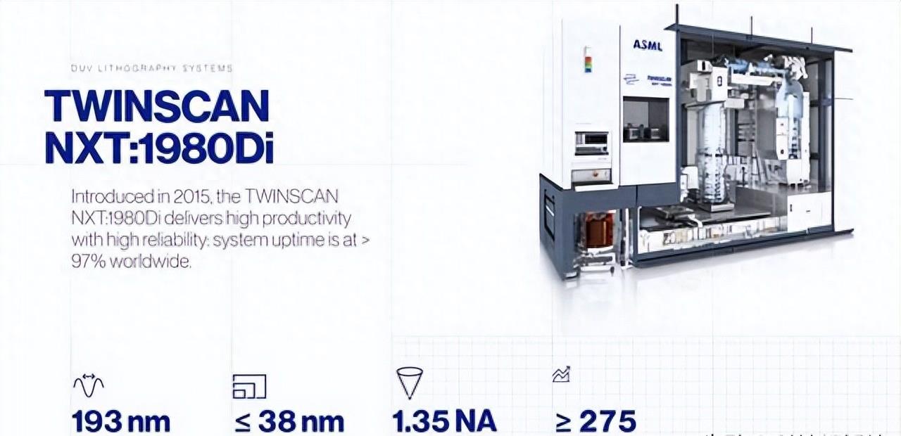
From the time frame, a prototype SMEE DUVi had been develop in 2019 with the goal of matching the performance of ASML NXT 1980i ( ICRD had a machine provided by ASML), along the way they had encounter difficulties but its part of a process and they had able to improve the machine with new upgrade. producing a new iteration that is able to match ASMLNXT 2000i, the whole process had taken two years from 2020 to 2022 by verification and validation. My thesis on 8-12 prototype build in 2022 with different configuration as new component are included after a major breakthrough like the light source from RS LASER, the rest is history.

DUVi has been developed in 2019, and mass production delivery will be confirmed by the end of the year​


Chinese scientists overcome the problem of lithography machines and reshape the technology industry. A story circulated on the Internet tells the story of Chinese scientific and technical personnel who were challenged by arrogant engineers during an inspection in Europe, but they later successfully overcame the problem of building lithography machines. The lithography machine is a kind of manufacturing equipment that requires very high precision, but Chinese scientific and technological personnel have overcome this problem with wisdom and diligence. Now, China has successfully manufactured a DUVi lithography machine with a resolution of 38 nanometers and can produce a 28-nanometer processor with a single exposure. The successful research and development of this technology reveals the momentum of China's technological innovation and progress, and will also have a profound impact on China's technology industry. According to official news, DUVi consists of four major systems: ArF light source, NA1.35 objective lens system, immersion system, and dual workpiece stage. China has now conquered all of them. Under the leadership of Chen Danian, an academician of the Chinese Academy of Sciences and director of the Institute of Microelectronics of the Chinese Academy of Sciences, China developed a lithography machine with a resolution of less than 28 nanometers in 2019. In November 2019, Chen Danian said that China is moving towards the goal of developing lithography machines with 14 nanometer, 7 nanometer or even lower process technology.

DUVi has been developed in 2019, and mass production delivery will be confirmed by the end of the year


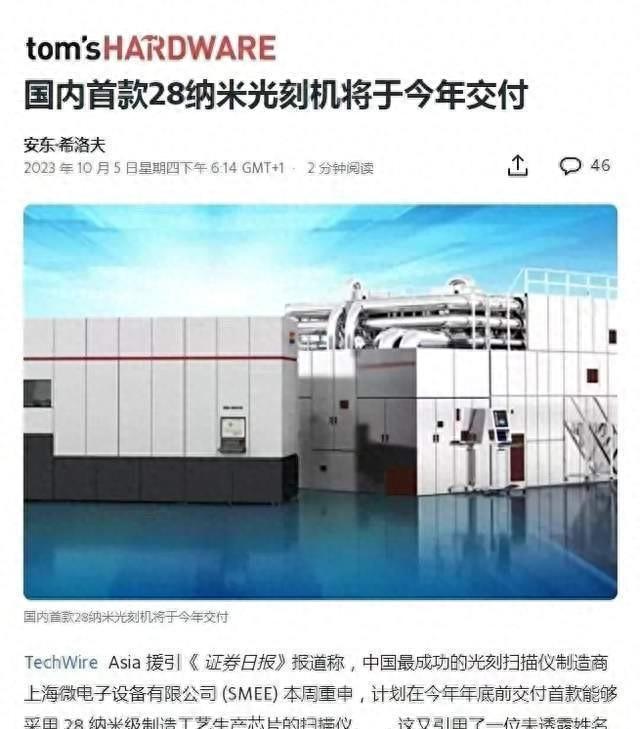
In May 2021, an engineer from Shanghai Microelectronics said in an interview with Nihon Keizai Shimbun that their main product is the lithography machine used for the 90nm process, and the yield rate of the lithography machine used for 28nm and 14nm chip production is still There is room for improvement. On October 5, 2023, TechWire Asia quoted the Securities Daily as reporting that Shanghai Microelectronics Equipment Co., Ltd. (SMEE), China's most successful lithography scanner manufacturer, plans to deliver its first 28-nanometer-scale scanner before the end of this year. Process production of chip scanners. The successful research and development of photolithography machines will have a profound impact on China's technology industry. It will enable Chinese companies to independently produce processors and other chips, reducing dependence on external technology. At the same time, this will also help improve China's global competitiveness and inject new vitality into China's scientific and technological innovation. However, it is also important to note that competition in technological innovation is not only based on the success of manufacturing technology, but also includes factors such as industrial ecology, talent flow, and policy support. Therefore, we need to think about how to more comprehensively improve the competitiveness of China's technology industry. Question: What impact do you think China's lithography machine technology research has on China's technological innovation?


DUVi has been developed in 2019, and mass production delivery will be confirmed by the end of the year
 

ansy1968

Brigadier
Registered Member
continue.....


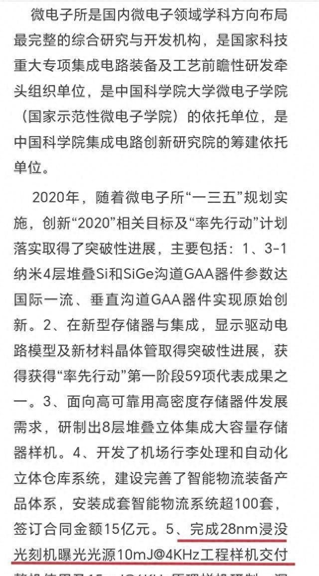
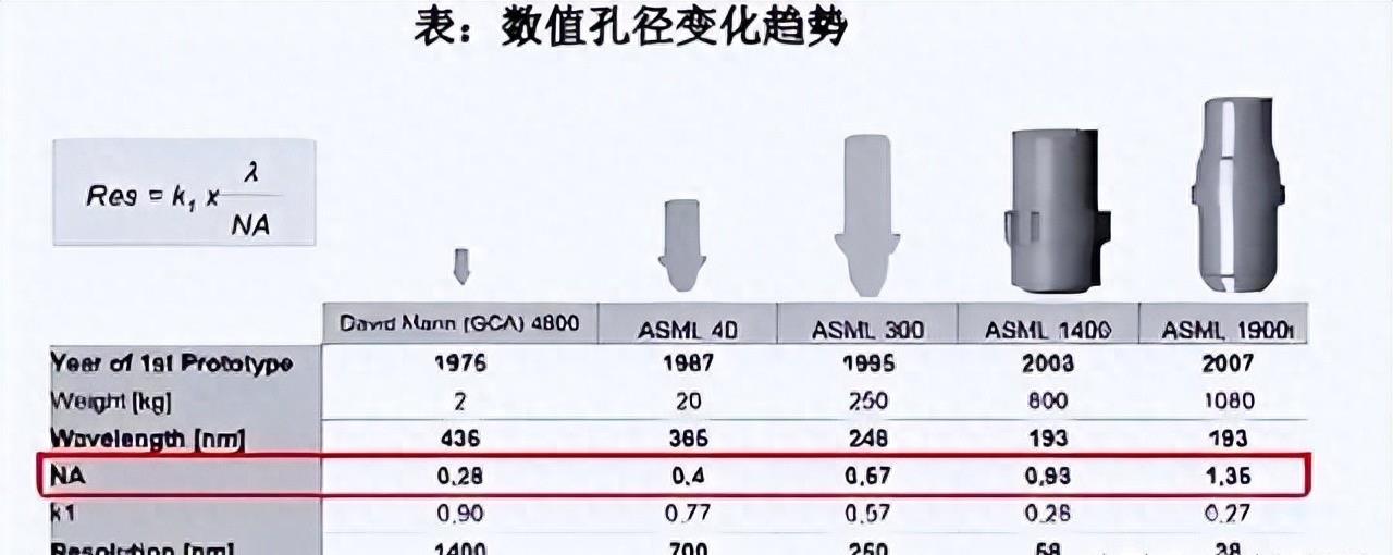
The Institute of Microelectronics of the Chinese Academy of Sciences revealed their latest achievements in the field of DUV exposure equipment in the 2022 yearbook. They completed the delivery of the 10mJ@4KHz engineering prototype of the 28nm immersion lithography machine exposure light source for complete machine use and the development of the 15mJ@6KHz principle prototype. This is a huge improvement and can support the 65-7nm process technology. Among them, the ArF light source with a maximum output power of 90W can realize the 5nm process technology. In addition, the NA value of the DUVi objective lens system needs to reach 1.35, which means that the aperture change trend of the objective lens must be guaranteed to be within the range of the high NA immersion optical system. Although the industrialization information of the NA1.35 objective lens system cannot be found in public information at present, the industrialization time is usually completed within 1-2 years. In addition, the immersion system is an indispensable part of the achievement transformation process, and acceptance must be completed before a huge investment can be made to establish a production line for mass production. It is reported that the official website of the People's Government of Lin'an District, Hangzhou City announced on September 7, 2018 that the main building of the Kaier Electromechanical Lithography Machine Immersion System Product Development Base has been capped. It is estimated that iterative improvement of production has been at least 2 generations. This means that the Institute of Microelectronics of the Chinese Academy of Sciences has huge potential in the field of DUV exposure equipment.

DUVi has been developed in 2019, and mass production delivery will be confirmed by the end of the year


DUVi has been developed in 2019, and mass production delivery will be confirmed by the end of the year


Title: The Institute of Microelectronics of the Chinese Academy of Sciences has achieved remarkable achievements in 2021, contributing greatly to the development of the microelectronics industry. Introduction: In recent years, the Institute of Microelectronics of the Chinese Academy of Sciences has achieved a series of remarkable achievements in the field of microelectronics, contributing greatly to the development of the microelectronics industry in China. made a huge contribution to its development. This article will sort out and summarize the achievements of the institute, showing its outstanding performance in technology research and development, project construction, etc. First paragraph: Looking back on 2021, the Institute of Microelectronics of the Chinese Academy of Sciences has made a series of important breakthroughs in the field of microelectronics. For example, they successfully developed a new type of microelectronic material with higher conductivity and lower energy consumption, which provides strong support for the rapid development of the microelectronics industry. Second paragraph: In addition to technology research and development, the Institute of Microelectronics of the Chinese Academy of Sciences also actively promotes project construction. They collaborated with the Hangzhou Lin'an District Committee to advance an important project that has made impressive progress in 2021. By investing hundreds of millions of yuan, a modern microelectronics production base has been built, which is expected to become an important support point for China's microelectronics industry.


DUVi has been developed in 2019, and mass production delivery will be confirmed by the end of the year


This technology uses the principle of laser interference to calculate the displacement of an object by measuring the phase difference of light waves. Compared with traditional measurement methods, it has higher accuracy and faster response speed. Whether it is tiny vibrations or high-speed movements, they can be accurately captured and measured. The application range of this technology is very wide. In the industrial field, it can be used to detect the deformation and displacement of mechanical parts to ensure the safe operation of equipment. In scientific research, it can be used to study the deformation characteristics and dynamic behavior of materials. In the medical field, it can be used to measure the expansion and contraction of human organs to help doctors perform precise diagnosis and surgery. Of course, to achieve precise displacement measurement, a high-quality instrument is essential. Currently, there are a variety of laser interference displacement measurement instruments available on the market. Their prices range from a few thousand yuan to hundreds of thousands of yuan, and they can meet customers with different needs. However, although this technology and instrumentation are very advanced in theory, there are still some challenges in practical application. For example, environmental factors such as changes in temperature and humidity can have an impact on measurement results. Furthermore, the sensitivity of the instrument may be limited for very small displacement amounts.
 

tokenanalyst

Brigadier
Registered Member

Chengdu High-tech Zone will introduce new policies to support the high-quality development of the integrated circuit industry​

The "Chengdu High-tech Industrial Development Zone's Several Policies on Supporting the High-quality Development of the Integrated Circuit Industry (Draft for Comments)" drafted by the Electronic Information Industry Bureau of Chengdu High-tech Zone was publicly solicited for opinions. The time is December 22, 2023 to January 23, 2024.
Integrated Circuit Design Policy

Article 1: Support enterprises to improve their R&D and design capabilities. Design companies that rent EDA tools provided by local R&D or national-level public service platforms will be given a subsidy of up to 1 million yuan based on 50% of the rental fee. For design companies that use multi-project wafers (MPW) for integrated circuit product development and tape-out, a subsidy of up to 5 million yuan will be provided based on 70% of the tape-out cost.
Article 2: Support enterprises to strengthen ecological cooperation. For companies that cooperate with local foundries to develop industrial software and IP cores, a subsidy of up to 2 million yuan will be provided based on 10% of the company's self-invested project research and development expenses. For design companies that carry out the first round of full-mask tape-out projects that are conducive to promoting the application of local integrated circuit line widths less than 45nm (inclusive) process production lines, a subsidy of up to 20 million yuan will be provided based on 50% of the tape-out cost, and subsequent mass production tape-outs will be provided. A subsidy of up to 5 million yuan per year for three years will be provided based on 5% of the tape-out cost. Design companies that use local packaging and testing services will be given a subsidy of up to 1 million yuan based on 15% of the increase in packaging and testing costs compared to the previous year.

Wafer manufacturing, packaging and testing policies
Article 3: Support enterprises to increase project investment. For newly introduced local integrated circuit companies with a total investment of less than 500 million yuan in integrated circuit wafer manufacturing, packaging and testing projects, and production line technology upgrades, and with fixed asset investments exceeding 10 million yuan, 8% of the actual investment in fixed assets will be granted The maximum subsidy is 20 million yuan, and the maximum subsidy amount for a single project shall not exceed 40 million yuan. For particularly major projects, support will be provided based on the principle of "one case, one discussion".
Article 4: Support enterprises to improve their manufacturing, packaging and testing service capabilities. For wafer manufacturing companies that provide tape-out foundry services for local design companies, a subsidy of up to 100 million yuan will be provided based on 8% of the foundry cost. For mass-produced packaging and testing companies that provide advanced packaging and high-reliability packaging and testing services to local design companies, a subsidy of up to 5 million yuan will be provided based on 5% of the packaging and testing costs; for newly put into production advanced packaging and high-reliability packaging products line, a subsidy of up to 5 million yuan will be provided based on 10% of the service order fee.

Equipment (parts), materials policy
Article 5: Accelerate the implementation of upstream and downstream supply chain projects. For new establishments or technological transformations in high-tech zones, as well as for the collaborative introduction and establishment of equipment (parts), materials and other supporting enterprises in cooperation parks in high-tech zones, and the investment in fixed assets exceeds 5 million yuan, a maximum of 1,000 yuan will be given based on 10% of the fixed asset investment amount. 10,000 yuan subsidy, and the maximum subsidy amount for a single project shall not exceed 20 million yuan. For particularly major projects, support will be provided based on the principle of "one case, one discussion".
Article 6: Support equipment and material verification applications. For integrated circuit companies that assist local and cooperative park companies to carry out verification of independent safe and controllable equipment (components), materials and other supporting products, a subsidy of 50% of the verification cost will be provided. The maximum cost for single equipment verification shall not exceed 1 million yuan, and each The maximum amount for verification of batch materials shall not exceed 500,000 yuan, and the maximum amount for each enterprise shall not exceed 10 million yuan. If the products of integrated circuit equipment (components) and materials companies enter well-known domestic and foreign companies for verification, a subsidy of no more than 20% of the entry verification cost will be provided, with a maximum subsidy of 5 million yuan. For local and cooperative park enterprises that successfully develop the first set (first batch) and achieve sales, a reward of up to 30 million yuan will be given based on 30% of the actual total sales of the product.
Article 7 supports supply chain collaboration. For integrated circuit companies that purchase equipment (parts), materials, industrial software and other products from local and cooperative park companies for the first time to form a supply chain, a subsidy of up to 5 million yuan will be provided based on 10% of the total purchase and sales contract (5% for both supply and demand parties); the amount For continued growth, a maximum subsidy of 5 million yuan will be provided based on 5% of the total purchase and sales contract (2.5% for both supply and demand sides), and the maximum subsidy amount for a single enterprise shall not exceed 20 million yuan per year.

Industrial Talent Introduction and Education Policy

Article 8: Support enterprises in hiring key talents. For IC design companies whose human resource costs exceed 500,000 yuan, and for manufacturing, packaging and testing, equipment (components), and materials companies whose human resource costs exceed 300,000 yuan, the company will be given the maximum annual maximum per person per year based on the efficiency of talent use. 500,000 yuan for talent performance rewards.
Article 9: Accelerate the cultivation of in-demand and applicable talents. For local enterprises that take the lead in building integrated circuit talent training bases with international and domestic universities and research institutes, a one-time subsidy of up to 5 million yuan will be given to the base based on 20% of the enterprise's construction investment cost. For local wafer manufacturing, packaging and testing companies that recruit fresh graduates and provide process technology instructional training for more than 6 months, a subsidy of 5,000 yuan per person and a maximum of 2 million yuan will be given to the company based on the actual number of employees retained after the training. Talent training; provide teaching subsidies of 10,000 yuan/year to tutors. For local enterprises that entrust professional training institutions to carry out training to improve the technical capabilities of engineers, a training subsidy of up to 500,000 yuan will be provided based on 20% of the actual training fees paid by the enterprise.

Industrial Ecological Leap Policy
Article 10: Support enterprises to become bigger and stronger. For IC design enterprises whose annual main business income exceeds RMB 100 million, RMB 300 million, RMB 500 million, or RMB 1 billion for the first time, one-time rewards of RMB 5 million, RMB 7 million, RMB 9 million, or RMB 11 million will be given in accordance with the principle of making up for the difference in promotion. ; For wafer manufacturing, packaging and testing enterprises whose annual main business income exceeds 300 million yuan, 500 million yuan, 1 billion yuan, or 2 billion yuan for the first time, they will be given 5 million yuan, 7 million yuan, or 9 million yuan in accordance with the principle of making up for the difference in the next grade. , a one-time reward of 11 million yuan; for equipment (parts) and materials companies whose annual integrated circuit-related main business income exceeds 50 million, 100 million, 300 million, or 500 million for the first time, 5 million yuan, One-time rewards of 7 million yuan, 9 million yuan and 11 million yuan. Enterprises are encouraged to use part of the above reward funds for personal rewards and subsidies for core managers, R&D personnel and other personnel who have made outstanding contributions.

Please, Log in or Register to view URLs content!
 

sunnymaxi

Captain
Registered Member
My thesis on 8-12 prototype build in 2022 with different configuration as new component are included after a major breakthrough like the light source from RS LASER, the rest is history.

i believe, this year production of Dry+Immersion lithography will remain stable. but from 2025 SMEE will increase production by many folds as Uprecision , Guowang and RSLaser expanding the capacity..
 

ansy1968

Brigadier
Registered Member
i believe, this year production of Dry+Immersion lithography will remain stable. but from 2025 SMEE will increase production by many folds as Uprecision , Guowang and RSLaser expanding the capacity..
2 to 3 units per month? so maybe 24 to 30 machine in 2024? again my hypothesis is based on SMIC receiving 2 brand new SSA800A late last year and may ramp up as component providers had finished their expansion plan in 2023/2024?
 

sunnymaxi

Captain
Registered Member
2 to 3 units per month? so maybe 24 to 30 machine in 2024? again my hypothesis is based on SMIC receiving 2 brand new SSA800A late last year and may ramp up as component providers had finished their expansion plan in 2023/2024?
UPrecision won 300+ million RMB order. so if we calculate per-set price, then total 20 units around. so it is safe to say that, they will finish expansion by this year. so next year production of lithography machines can ramp up.

as of March, 2023.. RSLaser have leased factory for production. they can produce 12 sets annually in that factory. so its now 10 months already. i believe this year they also finish new production facility.
 

ansy1968

Brigadier
Registered Member
13TH 5 year plan (2016-2020)

01 special project aircraft engine - check accomplished in late 2020.

02 special project DUVi -check finished development in 2019.

Both had been verified, validated and tested and will ready for mass production this year.

So My expectation for the 14th 5 year Plan(2020 -2025)

EUVi at the end of 2025.

7nm domestic line in late 2024/2025.

5nm chip in 2024 (ASML).
 
Last edited:

tokenanalyst

Brigadier
Registered Member

Ultra-thin Film Metrology Technique: Grazing Incident X-Ray Fluorescence​


Abstract:
Thickness measurements for a couple of atomic layer ultra-thin nitride and high-K dielectric materials (TaN, TiN, HfOx) were performed using our self-developed instrument, the ÅX- T100, via grazing incident x-ray fluorescence (GIXRF). Single-site repeatability results demonstrate that our instrument exhibits excellent precision with CV%=0.09%. An analysis of the wafer mapping results including 49 data points indicates a wafer thickness uniformity (uniformity %) of less than 3%. Considering the features of the x-ray fluorescence technique, which include non-invasiveness, immunity to surface oxidation, applicability to both metals and dielectrics, and suitability for transparent and opaque materials, GIXRF stands out as a perfect non-invasive metrology tool for measuring ultra-thin film thickness and composition at the angstrom level.​


Please, Log in or Register to view URLs content!


1704837211451.png
 
Top