Chinese semiconductor thread II

latenlazy

Brigadier
They did build chip on their own NPU architecture, but I haven’t seen any evidence with ascend 910 for example that it would have notable energy efficiency advantage over Nvidia chips.

I looked into it. H100’s peak power consumption is 700 watts. Ascend 910’s is 310 watts.

Please, Log in or Register to view URLs content!

Please, Log in or Register to view URLs content!
 

tokenanalyst

Brigadier
Registered Member

Tianyu Semiconductor's silicon carbide epitaxial project is about to start trial production​


According to the data, the total investment of the project is 8 billion yuan. It is located in Songshan Lake Ecological Park, with a total area of about 114.65 acres and a construction area of about 240,000 square meters. The construction content includes factory buildings, R&D buildings, dormitories and supporting facilities. After completion, it will be used to produce 6-inch/8-inch silicon carbide (SiC) epitaxial wafers with an annual production capacity of 1.5 million pieces. The construction period of the project is from 2023 to 2026, and the annual output value is expected to be about 10 billion yuan in the future.

As a SiC epitaxial wafer marketing, R&D and manufacturing company, Tianyu Semiconductor is the first company in China to achieve mass production of 6-inch SiC epitaxial wafers, thick epitaxial growth above 20kV level, n/p-type interface control technology such as gradual junction and steep junction, and multi-layer continuous epitaxial growth technology. In February 2023, Tianyu Semiconductor completed a round B financing of approximately RMB 1.2 billion. Investors include Haifu Industrial Fund, Guangdong Kexintai Equity Investment Fund, Nanchang Industrial Holdings, Jiayuan Technology, China Merchants Capital, Qianchuang Investment, etc. The funds from this round of financing will continue to be used to increase the expansion of SiC epitaxial production lines and continue to increase investment in the research and development of large-size SiC epitaxial growth.

Please, Log in or Register to view URLs content!
 

gelgoog

Lieutenant General
Registered Member
There are reasons why Nvidia chips still sell. Better chip interconnect speed & HBM3E availability among them.
I doubt the higher memory bandwidth will continue that far into the future. Given the way the US government has applied sanctions on chips with high interconnect performance expect the same with memory bandwidth eventually. It is also likely HBM sales to China will be sanctioned eventually.

On the other hand, if we agree that AI chip is more important than kirin chips, then why does huawei continue to use more wafers for the latter?
The Kirin chips are smaller in area so they can sell more of them. Probably better yields too.

Very doubtful that Huawei would have built their chip around a GPU based architecture since they don’t have any GPU products.
Actually Huawei do design and produce their own GPUs. The Maleoon GPU in the Kirin 9000S.
Not that this is relevant in this case since Huawei has dedicated NPU designs.
 

curiouscat

Junior Member
Registered Member
Doesn’t change the point?
Do you know what energy efficiency is? It’s not the maximum power consumption. It’s how much compute you can get per watt. It is extremely unlikely HUAWEI will match Nvidia on energy efficiency. They are still 2-3 node shrinks behind Nvidia. It is extremely difficult for any architectural change to compensate for being behind in node shrinks and even if it did it almost always comes at a cost at performance somewhere else.
Energy efficiency is not the issue here. China produces plenty of low cost energy. Think a little harder on why energy efficiency is important.
Energy efficiency is still a concern. The energy in China isn’t that cheap where we can just hand wave concerns away.

Please, Log in or Register to view URLs content!

More than half the cost from data centers in China come from power consumption and approximately 25% is coming from depreciation.
 

ansy1968

Brigadier
Registered Member
I'm surprise nobody post this YT, its very informative especially as the interviewee works in the semiconductor industry and know first hand what happening inside TSMC and the progress made in the Mainland. (he talks about a prototype EUVL, Photoresist, wafer vacuum and optical lens).

Please, Log in or Register to view URLs content!

Please, Log in or Register to view URLs content!

Please, Log in or Register to view URLs content!

Please, Log in or Register to view URLs content!


1.3K views1 day ago

Please, Log in or Register to view URLs content!

Please, Log in or Register to view URLs content!

In this episode of Strait Talk with Xiangyu, we explore the intricate world of semiconductors and geopolitics with a seasoned ...
 

tokenanalyst

Brigadier
Registered Member

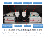
High-precision laser confocal measurement of semiconductor wafer thickness​

MIIT Key Laboratory of Complex-field Intelligent Exploration
Beijing Institute of Technology,School of Optics and Photonics​

Abstract​

Addressing the need for precise non-contact measurement of semiconductor wafer thickness, this study introduces a method based on laser confocal technology that ensures remarkable accuracy. It utilizes a voice coil nano displacement platform for high-resolution actuation of a laser confocal optical probe, enabling precise axial scanning. This method relies on identifying the peak points on the confocal laser's axial response curve, which are indicative of the objective lens's focal point, to accurately align and position the wafer's upper and lower surfaces. By accurately calculating the physical coordinates of each sampling point on the wafer surface through ray tracing algorithms, this technique achieves high-precision non-contact measurement of wafer thickness. A specialized laser confocal sensor for semiconductor wafer thickness measurement was developed, showing an axial resolution of under 5 nm, an axial scanning range of up to 5.7 mm, and repeatability in thickness measurement of under 100 nm across six wafer types. The process takes less than 400 ms for a single wafer. This research successfully applies confocal focusing technology to semiconductor measurement, offering a novel solution for high-precision, non-destructive, online wafer thickness measurement.​

1723650857486.png


Please, Log in or Register to view URLs content!
 

ZeEa5KPul

Colonel
Registered Member
I'm surprise nobody post this YT, its very informative especially as the interviewee works in the semiconductor industry and know first hand what happening inside TSMC and the progress made in the Mainland. (he talks about a prototype EUVL, Photoresist, wafer vacuum and optical lens).

Please, Log in or Register to view URLs content!

Please, Log in or Register to view URLs content!

Please, Log in or Register to view URLs content!

Please, Log in or Register to view URLs content!


1.3K views1 day ago

Please, Log in or Register to view URLs content!

Please, Log in or Register to view URLs content!

In this episode of Strait Talk with Xiangyu, we explore the intricate world of semiconductors and geopolitics with a seasoned ...
I saw this yesterday. Pretty meh overall, a fair bit of politics and the technical stuff isn't anything new to anyone who follows this thread, especially @tokenanalyst's patent posts.
 

tokenanalyst

Brigadier
Registered Member
I saw this yesterday. Pretty meh overall, a fair bit of politics and the technical stuff isn't anything new to anyone who follows this thread, especially @tokenanalyst's patent posts.
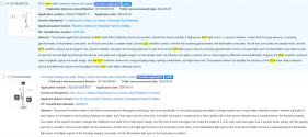
EUV photoresist patents are interesting but I would say is really impressive the quantity of EUV inspection tools patents that is coming out of China R&D institutions and companies, because that require EUV related tech like multilayer mirrors, vacuum tech, maglev stages, EUV light sources and EUV masks.

That means that China EUV lithography efforts are more advanced that some people think.
1723653993497.png
1723654110673.png
 
Top