Slightly off topic but most US tools are manufactured in the U.S. - KLA, Lam, TEL, and Applied all manufacture in the U.S. and they simply wouldn’t be captured in trade statisticsCompare that with the pathetic $12 billion USD per month chip tool purchases the US makes. And these are typically leading edge tools with much higher cost per unit and per wafer.
You are using an out of date browser. It may not display this or other websites correctly.
You should upgrade or use an alternative browser.
You should upgrade or use an alternative browser.
Chinese semiconductor thread II
- Thread starter vincent
- Start date
Slightly off topic but most US tools are manufactured in the U.S. - KLA, Lam, TEL, and Applied all manufacture in the U.S. and they simply wouldn’t be captured in trade statistics
They are made in mexico instead?
They are made in California, Texas, and MinnesotaThey are made in mexico instead?
IDK for the rest of the word but the vast majority of LAM, KLA and AMAT tools that are sold in China are made in huge manufacturing plants Singapore, Malaysia, Europe and so on.Slightly off topic but most US tools are manufactured in the U.S. - KLA, Lam, TEL, and Applied all manufacture in the U.S. and they simply wouldn’t be captured in trade statistics
Jiangsu Jinggong applies to expand 30 acres of silicon carbide related equipment production base
On August 11, according to Nantong Daily, Jiangsu Jinggong Semiconductor Equipment Co., Ltd. (hereinafter referred to as Jiangsu Jinggong), which is located in Qidong Economic Development Zone, Qidong City, Nantong City, Jiangsu Province, officially submitted an application to the park to build a 30-acre production base.It is reported that Jiangsu Jinggong plans to expand its production scale to further improve the production capacity and quality of core products such as wafer chamfering machines to meet the growing demand for high-end semiconductor equipment in domestic and foreign markets.According to official website information, Jiangsu Jinggong is committed to the research and development and manufacturing of semiconductor equipment.
It has independently developed 4-8 inch and 12 inch fully automatic chamfering machines, fully automatic wafer single-wafer cleaning machines, fully automatic wafer brushing machines, fully automatic waxing machines and profilometers, etc.In the field of large silicon wafers, Jiangsu Jinggong has successfully launched 12-inch wafer chamfering equipment and technical solutions, effectively solving the problem of large-size silicon wafer processing. At the same time, in the field of third-generation semiconductor material silicon carbide, Jiangsu Jinggong focuses on providing chamfering, cleaning equipment and supporting processes for 6-inch, 8-inch and non-standard diameter silicon carbide substrates.

At present, Jiangsu Jinggong has applied for 19 product-related patents through industry-university-research cooperation with Shandong University and others, and has obtained 1 authorized invention patent and 4 utility model patents. The 12-inch fully automatic chamfering machine MET-5800 developed by it has broken the domestic monopoly of imported large silicon wafer chamfering machines, and the fully automatic chamfering machine MET-5600 has successfully replaced the chamfering machines imported from Japan.In terms of the market, Jiangsu Jinggong has signed a contract with a well-known European substrate manufacturer for a fully automatic wafer chamfering machine, marking the beginning of Jiangsu Jinggong's products going abroad.
It has independently developed 4-8 inch and 12 inch fully automatic chamfering machines, fully automatic wafer single-wafer cleaning machines, fully automatic wafer brushing machines, fully automatic waxing machines and profilometers, etc.In the field of large silicon wafers, Jiangsu Jinggong has successfully launched 12-inch wafer chamfering equipment and technical solutions, effectively solving the problem of large-size silicon wafer processing. At the same time, in the field of third-generation semiconductor material silicon carbide, Jiangsu Jinggong focuses on providing chamfering, cleaning equipment and supporting processes for 6-inch, 8-inch and non-standard diameter silicon carbide substrates.

At present, Jiangsu Jinggong has applied for 19 product-related patents through industry-university-research cooperation with Shandong University and others, and has obtained 1 authorized invention patent and 4 utility model patents. The 12-inch fully automatic chamfering machine MET-5800 developed by it has broken the domestic monopoly of imported large silicon wafer chamfering machines, and the fully automatic chamfering machine MET-5600 has successfully replaced the chamfering machines imported from Japan.In terms of the market, Jiangsu Jinggong has signed a contract with a well-known European substrate manufacturer for a fully automatic wafer chamfering machine, marking the beginning of Jiangsu Jinggong's products going abroad.
Changdian Technology: Acquisition of 80% equity interest in SanDisk Semiconductor approved
On August 11, Changdian Technology issued an evening announcement stating that the company's fifth extraordinary meeting of the eighth board of directors held on March 4, 2024 reviewed and approved the "Proposal on the Acquisition of 80% of the Equity of SanDisk Semiconductor (Shanghai) Co., Ltd. by Changdian Technology Management Co., Ltd., a wholly-owned subsidiary of the company, and agreed that Changdian Technology Management Co., Ltd. would acquire 80% of the equity of SanDisk Semiconductor (Shanghai) Co., Ltd. held by SANDISKCHINA LIMITED in cash. The transaction price is approximately US$624 million (approximately RMB 4.473 billion).
Recently, the acquisition case has made new progress. SanDisk Semiconductor has received a letter of consent issued by the Minhang District Planning and Natural Resources Bureau of Shanghai (Min Planning and Resources Bureau [2024] No. 47), agreeing to the proposed equity change in this transaction, that is, the shareholder and investment ratio of SanDisk Semiconductor will be changed from SanDisk China Limited holding 100% to Changdian Technology Management Co., Ltd. holding 80% and SanDisk China Limited holding 20%.
At the same time, Changdian Technology has received the "Decision on Non-Prohibition of Anti-Monopoly Review of Operator Concentration" issued by the State Administration for Market Regulation, which decides not to prohibit the transaction and all parties to the transaction can continue to move forward.
Changdian Technology has stated that the acquisition is based on in-depth analysis and forward-looking judgment of the global storage market, and aims to expand the company's market share in the storage and computing electronics fields. It is understood that SanDisk Semiconductor was established in 2006 and is mainly engaged in the packaging and testing of advanced flash storage products, including iNAND flash memory modules. Its parent company Western Digital is a leading global memory manufacturer. It has established a long-term cooperative relationship with Changdian Technology since 2003 and is one of its important customers.
Fudan team achieves large-scale integration and extreme miniaturization of ultra-fast flash memory for the first time
The rapid development of artificial intelligence urgently requires high-speed non-volatile storage technology. The current mainstream non-volatile flash memory has a programming speed of hundreds of microseconds, which cannot support application needs. The preliminary research of the Zhou Peng-Liu Chunsen team at Fudan University showed that two-dimensional semiconductor structures can increase the speed by more than a thousand times, achieving disruptive nanosecond-level ultra-fast storage flash memory. However, how to achieve large-scale integration and move towards practical application is extremely challenging.

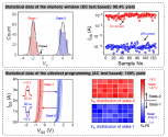
Starting from interface engineering, the team verified the integration verification of 1kb ultrafast flash memory array for the first time in the world, and proved that the ultrafast characteristics can be extended to sub-10 nanometers. At 5 pm Beijing time on August 12, the relevant results were published in the international top journal Nature Electronics under the title " A scalable integration process for ultrafast.
The team developed super-interface engineering technology, realized heterogeneous interfaces with atomic-level flatness in large-scale two-dimensional flash memory, and combined with atomic-level precision characterization technology, verified that the integrated process is significantly better than the international level. Through strict DC storage window and AC pulse storage performance tests, it was confirmed that the yield of two-dimensional flash memory is as high as 98% at nanosecond non-volatile programming speed in a 1Kb storage scale, which is higher than the 89.5% yield requirement for flash memory manufacturing in the International Technology Roadmap for Semiconductors.
At the same time, the research team developed a self-aligned process that does not rely on advanced lithography equipment. Combined with the original innovative ultrafast storage stacked electric field design theory, they successfully realized an ultrafast flash memory device with a channel length of 8 nanometers, which is currently the shortest channel flash memory device and has broken through the physical size limit of silicon-based flash memory (about 15 nanometers). Supported by an atomically thin channel, this ultra-small device has 20 nanosecond ultrafast programming, 10 years of non-volatility, 100,000 cycle life, and polymorphic storage performance. It is expected to promote the industrialization of ultrafast disruptive flash memory technology.
The first domestically produced large-size ECD equipment was launched, and glass substrate manufacturing technology
Xinju (Shenzhen) Semiconductor Technology Co., Ltd. was established in June 2020. The core team is from Europe. It is a high-tech enterprise dedicated to the field of advanced integrated circuit manufacturing. Xinju Semiconductor focuses on the research and development and production of electrochemical deposition (ECD), etching process and micropore processing equipment, providing domestic and foreign customers with the most advanced domestic complete sets of technical equipment and complete sets of technical services.
As an enterprise that has been recognized by many institutions, including "National High-tech Enterprise", "Shenzhen Major Project Plan" and "Shenzhen Specialized and New Enterprise", Xinju Semiconductor's wet process equipment has achieved internationally leading process performance and indicators, while realizing independent intellectual property rights and a high degree of localization. It is not dependent on and restricted by foreign technology, and can solve the commercial mass production and application of various high-density packaging substrates (such as xBF-ICS, TGV glass substrates), microLED displays and new generation substrate materials that are currently in urgent need of 2.5D advanced packaging, helping China to take the lead in the semiconductor field and the new generation of information technology.
At present, the company's high-performance ECD equipment has the ability to fill TGV holes with a high yield of 1:15 aspect ratio, and the mass production manufacturing capability of ultra-fine and ultra-thin RDL graphic lines with a line width/line spacing of less than 5 microns. Through hundreds of actual machine proofing by downstream customers, it has been recognized by customers and has accumulated a large amount of key process technology data required for the commercial mass production of glass substrates. The results and data prove that this equipment has completely broken the foreign technology monopoly and reached the international leading technology level.
At the same time, based on the company's own core patents, Xinju has developed key technologies such as ReverseStream, AVC and Maglev to achieve mass production of glass substrates, which can effectively prevent the problems of fragmentation and consistency encountered in the current industry during batch manufacturing, and provide a solid foundation for the commercial manufacturing of domestic glass substrates.

If Huawei's Ascend 910C truly has comparable performance to H100's, then US strategy of offering crippled H100s (i.e., H20s) has objectively and completely backfired. US wants to keep a foot in the door in the second largest AI market, yet inadvertently ceded the entire market to Huawei monopoly with its outdated and draconian sanction regime. It's truly a gift that keeps on giving. The cherry on top is that generative AI and LLMs have remarkably little-to-zero discernible military implications. So economically and militarily, you really have to question how US got so arrogant to believe they can simply stop AI development in China.
