Chinese semiconductor thread II

tokenanalyst

Brigadier
Registered Member

Koala Youran officially completed shipment of China's first glass-based Micro LED wafer quality inspection equipment​


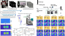
The first domestic glass-based Micro LED wafer mass detection equipment independently developed by Koala Youran has officially completed shipments recently. This indicates that Koala Youran has completed the technical research and development of the product and has been recognized by customers, and has the ability to mass-produce Micro LED wafer mass detection equipment. The product has the characteristics of high precision, high stability, and high efficiency.

According to Koala Youran, in addition to appearance inspection, Micro LED wafer inspection also requires accurate measurement of chip rotation to meet the core quality requirements of Micro LED wafers. The glass-based Micro LED wafer inspection equipment developed by it integrates internationally advanced technology and its independently developed core algorithm, and has the characteristics of high precision, high stability, and high efficiency.

The device adopts a high-precision adjustable magnification optical system with a 20X optical accuracy of up to 0.16um. Combined with the company's self-developed "active learning" AI algorithm, it can not only accurately identify appearance defects, but also accurately classify defects.

In terms of deviation measurement, Koala Youran eliminates system errors caused by factors such as motion and distortion through calibration and coordinate system conversion, ensuring the high accuracy of deviation measurement. The measurement error under standard film testing is controlled within ±0.5um.

Please, Log in or Register to view URLs content!
 

gelgoog

Lieutenant General
Registered Member
From my understanding Japan has had the technology to build EUV for a while if they wanted to. They didn’t because economically ASML effectively beat them to it. China wouldn’t be building EUV at all if the sanctions didn’t force them. It’s a total waste of money when that money could’ve be invested into other projects and sectors that have higher ROI. Unfortunately China doesn’t have a choice.
ASML got billions of funding from Intel, TSMC, Samsung.
Please, Log in or Register to view URLs content!

Nikon did not get that kind of funding.

The Japanese did not even have FinFET fabs with 16nm process or better. So no demand there. And their major foreign client, Intel, paid ASML to build an EUV tool. No demand there either.

This was in part done on purpose by the EU and the US governments to push the Japanese vendors out of the lithography segment.

I think I said this before but China should try to push for 450mm wafers. They would get increased economies of scale and their market is large enough to pay for it.
 

FairAndUnbiased

Brigadier
Registered Member
ASML got billions of funding from Intel, TSMC, Samsung.
Please, Log in or Register to view URLs content!

Nikon did not get that kind of funding.

The Japanese did not even have FinFET fabs with 16nm process or better. So no demand there. And their major foreign client, Intel, paid ASML to build an EUV tool. No demand there either.

This was in part done on purpose by the EU and the US governments to push the Japanese vendors out of the lithography segment.

I think I said this before but China should try to push for 450mm wafers. They would get increased economies of scale and their market is large enough to pay for it.
450 mm wafer will require huge changes in the entire workflow due to increased chamber size. Lots of semiconductor equipment engineering challenges for uniform gas delivery and plasma generation. More expensive pumps.
 

tokenanalyst

Brigadier
Registered Member
450 mm wafer will require huge changes in the entire workflow due to increased chamber size. Lots of semiconductor equipment engineering challenges for uniform gas delivery and plasma generation. More expensive pumps.
I think the main killer issue for 450mm will be lithography because is the "machine that moves", will take a lot more time to pattern the wafer. Probably ion implantation too but not as a bigger deal as lithography.
 

tokenanalyst

Brigadier
Registered Member

Mask defect detection by combining wiener deconvolution and illumination optimization.​


Institute of Advanced Science Facilities, Shenzhen.
State Key Laboratory of Optoelectronic Materials & Technology, School of Physics, Sun Yat-sen University.
Center for Neutron Science and Technology, Guangdong Provincial Key Laboratory of Magnetoelectric Physics and Devices.​

Abstract​

In the lithography process, mask defect is inevitably replicated on chips hence the yield and quality of the product are directly related to the mask quality. Mask microscopy resolution is then an essential specification. In this work, a high-efficiency method for enhancing the resolution of mask defect is proposed based on illumination optimization and Wiener deconvolution. To validate this approach, we established a verification apparatus designed to achieve a theoretical resolution of 3.0 μm with visible light. Remarkably, the empirical results demonstrated that the actual resolution attained is as low as 2.5 μm. The verification demonstrates a significant improvement for various periodic fringes. Moreover, the augmented capability of the apparatus facilitates the identification of mask defects. Although the experiment is carried out for the visible wavelength, the research is specifically designed for the working conditions suitable for EUV mask detection based on the preparatory work for the EUV.

1723071892493.png

Please, Log in or Register to view URLs content!
 

latenlazy

Brigadier
Some comment said ASML had considered and rejected this type of settings

because it's much cheaper and easy to make, they cannot charge customers high prices so big no-no?
No. This simplified setup requires extremely precise alignments and I wouldn't be surprised if it demands very restrictive tolerances for the beam properties of the light source as well. No one employs higher element optical systems if they can get away with a lower element one. You go with higher element if it gives you more degrees of control to adjust the beam into an ideal profile, and general robustness with the quality of the light beam you're trying to project, and only go as high as absolutely necessary. I'm sure the design for this specific projection system from Japan tries to account for those requirements, but anytime you are employing a design with less forgiving tolerances there's a chance that the approach doesn't pan out reliably in practice.
 

gelgoog

Lieutenant General
Registered Member
Please, Log in or Register to view URLs content!
AMEC inaugurated a 140,000 sq meters production site in Lingang, Shanghai.

For comparison the main Lam Research site at Tualatin in the US is 600,000 sq feet (under 56,000 sq meters). Their Malaysian production site is 800,000 sq feet (slightly over 74,000 sq meters).

AMEC is also currently building a 100,000 sq meters R&D and HQ site.

For comparison Lam Research a decade ago had like 161,000 sq feet at their Fremont R&D and HQ site. And they were building another 134,000 sq feet. Over 27,000 sq meters total once all construction was done.

AMEC also claim they will grow their facilities to 440,000 sq meters in area total in the future. That is yuge.

I think the main killer issue for 450mm will be lithography because is the "machine that moves", will take a lot more time to pattern the wafer. Probably ion implantation too but not as a bigger deal as lithography.
You increase the power of the light source. And then the time goes down. I know that Gigaphoton for example has higher power light sources they developed for 450mm which are not used in any current Nikon machine.
 
Last edited:

tokenanalyst

Brigadier
Registered Member
You increase the power of the light source. And then the time goes down. I know that Gigaphoton for example has higher power light sources they developed for 450mm which are not used in any current Nikon machine.
The light source is one the problems but there is also the wafer stage worktable that to even to keep up with current 300 mm performance will have to accelerate way faster, causing issues of vibration and accuracy. Then there is the overlay performance, for a 450mm you have to add more marks and find them faster than with 300 mm wafers.

The change on lithography just to have a performance closer to 300 mm would have been more drastic than with any other manufacturing equipment. That is the one of the main reasons why 450mm was abandoned.
 

siegecrossbow

General
Staff member
Super Moderator
American sanctions and export controls are backfiring:
everybody, friend and foe, wants to de-Americanize its products,
to be not a victim of American sanctions and export controls on products containing any American technology.
See also:
Please, Log in or Register to view URLs content!

This isn’t so much shooting themselves in the foot as shooting themselves in the balls. What were they thinking…
 
Top