Chinese semiconductor thread II

GiantPanda

Junior Member
Registered Member
American sanctions and export controls are backfiring:
everybody, friend and foe, wants to de-Americanize its products,
to be not a victim of American sanctions and export controls on products containing any American technology.
See also:
Please, Log in or Register to view URLs content!

The gamechanger for this would be if Japan gives the greenlight to export the new EUV to China.

This would give Japan a near monopoly for high-end foreign litho gear in China (along with local ptoducts from SMEE, CIOMP, etc) and put massive pressure on ASML to de-Americanize as well.

If ASML de-US-izes, well then that would put the final nail in the coffin for the US chip-ban diktat as well as the US chip industry.

But all this depends on Japan acting independently for its own interests which is not a given.
 

sunnymaxi

Captain
Registered Member
The gamechanger for this would be if Japan gives the greenlight to export the new EUV to China.
that was a research from Okinawa University professor .. it will take time if they decide to produce prototype from research then long testing process and production. need financial backing as well..

so its too early to talk about this..

by that time, China's own EUV will come online.. CIOMP is about to deliver first prototype.
 

Weaasel

Senior Member
Registered Member
I had to shake my head at that quote. The impact of sanctioning software companies like this can be disruptive but far different from sanctioning companies that rely on physical supply chains to make things.

And no, they don't actually decide to put companies on the entity list depending on how much they're impacted by it. At best, it's a signaling mechanism even if the specific impact is more of an inconvenience after the disruption or they're just going down the list regardless.

I swear that was an answer you'll get if you plug a question into chatgpt.
Words put together that don't make much sense in context if you have a passing familiarity with the topic....
I was thinking so myself...
 

tokenanalyst

Brigadier
Registered Member
New metrology company from people with experience in KLA.

Semiconductor Overlay Engraving Equipment "Ariva Semiconductor" Completed Pre-A Round with 3 Rounds of Financing in 7 Months​


Recently, Aerwei Semiconductor, a semiconductor core production line equipment and semiconductor overlay equipment provider, completed its Pre-A round of financing, with joint investment from Zhuoyuan Asia and Jinyu Maowu. This is the third round of financing in 7 months, following the seed + round of Source Code Capital, Xiangfeng Changqing, Zhuoyuan Asia, Xi Venture Capital, and Small and Medium Enterprise Development Fund in January 2024; and Jinyu Maowu, Source Code Capital, and Zhuoyuan Asia in March 2024.

It is understood that the founding team of "Are Micro Semiconductor" comes from top product and R&D institutions such as KLA Shanghai R&D Center, Institute of Microelectronics of the Chinese Academy of Sciences, and Department of Precision Instruments of Tsinghua University. It is one of the few established teams of overlay equipment in Asia and has undertaken the research and development of many major national special projects. "Are Micro Semiconductor" founder and CEO Duan Hongwei comes from KLA Shanghai R&D Center, and CTO Dr. Gai Hongfeng is a Ph.D. from the Department of Precision Instruments of Tsinghua University. He was a researcher at the Institute of Microelectronics of the Chinese Academy of Sciences. He is a domestic core team with more than 20 years of R&D and mass production experience.

The mass production equipment developed by the "Eruiwei Semiconductor" team can meet the support needs of almost all wafer fabs in the mainland in the next 15 years, especially for the overlay needs of advanced processes below 16nm. The team has mass-produced in TSMC, Samsung and other international leading wafer fabs.​
 

pbd456

Junior Member
Registered Member
If Japan wants to build EUV, it would have built it. The light source was developed years ago, they obviously have stage table for 5nm DUV.
 

ansy1968

Brigadier
Registered Member
If Japan wants to build EUV, it would have built it. The light source was developed years ago, they obviously have stage table for 5nm DUV.
You forget to include EUV photoresist, all the building blocks are there except of course the design and fabrication of 7nm, 5nm and 3nm tech node.
 

tokenanalyst

Brigadier
Registered Member
Different from what some stooges think, metrology is one the fastest growing equipment sectors in China.

Tianjue Technology (TZTEK): China's first 40NMBFI released, semiconductor layout ushered in new breakthroughs​


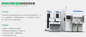
Tianjue Technology announced on its official account that Suzhou Sihang Semiconductor Technology Co., Ltd. (hereinafter referred to as "Sihang Semiconductor"), in which it holds a stake, has completed in-factory verification of its bright-field nano-pattern wafer defect detection equipment TB1500 for the 40nm technology node, marking a new breakthrough in domestic high-end semiconductor detection equipment.

  Defect detection equipment is an important tool for chip quality improvement, cost reduction, and iteration: In chip manufacturing, from the entire wafer to a single chip, defect detection equipment is an important tool for chip quality improvement, cost reduction, and iteration. The

  TB1500 announced this time is another breakthrough following the TB1000 in August last year. All core key components are independently controllable. At the same time, advanced signal processing algorithms are used to effectively improve the signal-to-noise ratio and detection sensitivity to meet the process requirements of the 40nm technology node. The TB2000 equipment for the 28nm technology node is currently progressing smoothly, and all core components have been developed. It is planned to release a prototype by the end of 2024.

  The semiconductor layout has blossomed in many places, and the new product iteration of wholly-owned subsidiaries has also progressed smoothly: the DaVinci G5 equipment developed by wholly-owned subsidiary MueTec for the 12-inch 40nm technology node has been verified by a large amount of wafer actual measurement data and has performed well. The equipment improves the repeatability, throughput and high aspect ratio overlay mark recognition capabilities, making it possible to detect the overlay accuracy of complex chip patterns and improving manufacturing efficiency.

1723042929646.png

Please, Log in or Register to view URLs content!
 

tokenanalyst

Brigadier
Registered Member

AMEC celebrates its fifth anniversary of listing on the Science and Technology Innovation Board​


AMEC insists on high-quality development, solid progress in technological progress, business development, performance growth, standardized governance, etc., and its comprehensive competitiveness continues to improve, and a series of breakthrough progress and achievements have been made.

• As of June 2024 , the company has accumulated 5,164 reaction tables in mass production and large-scale repetitive sales on 131 production lines at home and abroad ;

• As of June 2024 , the company has applied for 2,648 patents, including 2,224 invention patents ;

• As of June 2024 , the company has 2,085 employees , of which 46.38% are R&D personnel , a year - on-year increase of 188% in the number of employees ;

• In 2023 , the company's operating income and net profit attributable to shareholders of the parent company both hit record highs, reaching 6.264 billion yuan and 1.786 billion yuan respectively, which are 3 times and 9 times the sales and profits in 2019 ;

• It has won more than 100 well-known awards in the fields of science and technology, customer satisfaction, intellectual property, quality certification, etc., and has been ranked among the top in the US TechInsights global customer satisfaction rating for many years.


Focus on key integrated circuit equipment and continuously improve product innovation capabilities

AMEC attaches great importance to the innovation of core technologies, always emphasizes innovation and differentiation and maintains high-intensity R&D investment, and is committed to developing high-end micro-processing equipment. By creating internationally competitive technological innovations and differentiated products, AMEC provides customers and the market with equipment solutions with superior performance, high production efficiency and high cost performance. As of June 2024 , the company has a total of 5,164 reaction tables and 131 production lines in China, Asia and Europe, fully realizing mass production and a large number of repetitive sales, and has won the trust and support of many customers and suppliers.

With the industry's first dual-machine etching equipment technology, AMEC took the lead in proposing the concept of "picometer-level" processing accuracy. Its etching accuracy has reached below 100 " picometers " , equivalent to 1/3.5 million of a human hair . In addition, the product has the advantages of rich etching application coverage, which can meet more than 90% of etching application needs, and its technical capabilities have covered more advanced levels of 5 nanometers and below. The company's new orders in 2023 will amount to approximately 8.36 billion yuan, a year-on-year increase of approximately 32.3% , of which new orders for etching equipment will be approximately 6.95 billion yuan, a year-on-year increase of approximately 60.1% .

AMEC continues to increase its investment in innovation and research and development, making breakthroughs in the field of semiconductor thin film deposition equipment, launching a number of new products such as Preforma Uniflex® CW , Preforma Uniflex® HW , and Preforma Uniflex® AW to meet market demand, providing strong growth momentum for the company's diversified business development. In addition, the company's newly developed silicon and silicon germanium epitaxial EPI equipment, wafer edge Bevel etching equipment and other new products will also be put into the market for verification in the near future.


In terms of MOCVD technology, since the launch of the first generation of MOCVD equipment PRISMO A7® , AMEC has continuously enriched its product line and rapidly upgraded and iterated. At present, AMEC has a stable market share in the field of GaN-based equipment such as Mini LED , and continues to develop MOCVD equipment for GaN, SiC and other power devices and Micro-LED device manufacturing . In addition, AMEC has also invested in the fourth largest equipment market - optical inspection equipment.

Please, Log in or Register to view URLs content!
 

tokenanalyst

Brigadier
Registered Member

AMEC opens Shanghai Lingang industrialization base​


On August 2, China's semiconductor equipment company AMEC announced that its Shanghai Lingang Industrialization Base was officially opened. It is reported that the base covers an area of about 157 acres and a total construction area of about 180,000 square meters. It adopts an advanced factory management system and is equipped with an intelligent three-dimensional warehouse, which realizes the tracking of manufacturing resources and the monitoring of the production process, which can improve production quality and efficiency, reduce production costs, and lay the foundation for ensuring the supply of global customers.

With the full commissioning of the Lingang industrialization base, AMEC's future development blueprint is slowly unfolding. In July 2023, AMEC's production and R&D base in Nanchang, Jiangxi Province was completed and put into use; the AMEC Lingang headquarters and R&D building located on the shore of Dishui Lake in Shanghai is also under construction, covering an area of about 100,000 square meters after completion. In the future, the total area of AMEC's production and R&D base will reach about 450,000 square meters.

Since its development, AMEC has continuously developed market-competitive equipment with high-end semiconductor equipment as its core. The company is also integrating upstream and downstream of the industry chain and related resources to promote faster development of the company. AMEC expects that in the next five to ten years, it will cover 50% to 60% of the equipment in the key fields of integrated circuits through independent research and development and cooperation with industry partners.​
Please, Log in or Register to view URLs content!
 

curiouscat

Junior Member
Registered Member
You forget to include EUV photoresist, all the building blocks are there except of course the design and fabrication of 7nm, 5nm and 3nm tech node.
From my understanding Japan has had the technology to build EUV for a while if they wanted to. They didn’t because economically ASML effectively beat them to it. China wouldn’t be building EUV at all if the sanctions didn’t force them. It’s a total waste of money when that money could’ve be invested into other projects and sectors that have higher ROI. Unfortunately China doesn’t have a choice.
 
Top