Chinese semiconductor thread II

tokenanalyst

Brigadier
Registered Member

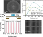
Feasibility study of fabricating 20 nm resolution dielectric Fresnel zone plates with ultrahigh aspect ratio for EUV optics.​

Nanolithography and Application Research Group, School of Information Science and Technology, Fudan University, Shanghai, China
Shanghai Key Laboratory of Metasurfaces for Light Manipulation, Fudan University, Shanghai, China.

Abstract​

EUV light optics are either reflective or diffractive due to the substantial absorption characteristics by almost all materials. Despite great successes in manufacturing integrated circuit chips, reflective EUV optics are still unfriendly to small-to-medium enterprise (SME) because of the enormous costs. Recently, diffractive EUV optics has come to the light in hopes to be able to establish manufacturing nanoscale products and inspecting nanoscale structures. Diffractive zone plates with high resolution in EUV wavelengths are urgently needed. This paper reports our latest success in developing 20 nm resolution zone plates for focusing and imaging in the EUV and soft X-ray regions. It firstly discusses the diffraction efficiency of FZPs tailored for 13.5 nm wavelength to decide the essential height of the zone plate. Then, Monte Carlo simulation method was used to figure out the achievable zone plate parameters by high-resolution electron beam lithography (EBL). Finally, this work systematically explored the viability of nanofabricating top-tier 20 nm resolution hydrogen silsesquioxane (HSQ) zone plates with the duty cycle ratio nearing 1:1 and the aspect ratio approaching 13:1 on 50 nm thick Si3N4 membranes.
1719242529641.png

Please, Log in or Register to view URLs content!
 

LanceD23

New Member
Registered Member
What's the source for that?
lol, source? to prevent US from finding out on China lithography development, no official source can reveal anything about that. It's top secret. Everything taken down from offical news channel.
It will be a blackbox model, as Huawei chips continously churning out in forseable future. US officials banking on no service for ASML machines and no sale useable chemcials means one day CHina will be ground to a halt.
If that doesn't happen in future, then it means US missed out on China own lithography development.
so, you can tell by whether huawei got stopped one day.
 

tokenanalyst

Brigadier
Registered Member
AI takeover Chinese fabs: Interesting Naura patent for using machine learning models to accurate control the temperature gradient of their etching and deposition equipment. An AI model can in theory force its way to replicate more stringent lab conditions in a fab setting and an AI model can improve itself.

Wafer etching or deposition and model acquisition method, semiconductor process equipment​

CN117637554A​

Beijing Naura Microelectronics Equipment Co Ltd

Abstract​

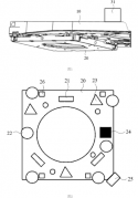
The embodiment of the present invention discloses a wafer etching or deposition and model acquisition method, and semiconductor process equipment, and specifically relates to a temperature control method for each temperature control zone of a multi-temperature zone electrostatic chuck or a heating base. The temperature control method combines the influence of temperature sensitivity and the diffusion distribution of etching byproducts or deposits along the temperature gradient on the etching or deposition rate, and can more accurately predict the etching or deposition rate distribution data of each position on the wafer at any target temperature of each temperature control zone, or according to the target etching or deposition rate distribution data, by adjusting the target temperature control value of each temperature control zone, so as to improve the uniformity of wafer etching or deposition, or make the wafer surface obtain the desired morphology.​


1719243458276.png
 

tokenanalyst

Brigadier
Registered Member

Grating measurement module vibration reduction devices, test systems and test benches.​

Beijing U Precision Tech Co Ltd

CN118110755A​

Abstract​

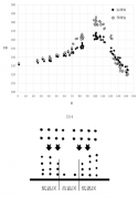
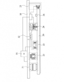
The present invention provides a grating measurement module vibration reduction device, a grating measurement module vibration reduction test system and a damper offline test bench, which relate to the field of grating measurement technology, and solve the problem of effectively reducing the influence of external vibration on a grating mounting plate. The grating measurement module vibration reduction device comprises a grating mounting plate, and a flexible block, a vibration reduction damping and a stiffness damping connected to the grating mounting plate. The vibration reduction damping, the flexible block and the stiffness damping are respectively evenly distributed on the same side of the grating mounting plate, and the flexible block and the stiffness damping are alternately arranged. The grating mounting plate can be improved in structural stability within the resonant frequency range.​

1719246580603.png1719246593635.png
 

LanceD23

New Member
Registered Member
At least caveat your statement then if there isn't an official source. Don't be a tool
Its aggregrate of various online snippets and then make a judgement on that and making connections with what's public known
western source
1)Huawei has established a official lithography division in shanghai
2)28nm scanner to be delivered by 2023 year end


Please, Log in or Register to view URLs content!

Please, Log in or Register to view URLs content!

Please, Log in or Register to view URLs content!

Please, Log in or Register to view URLs content!


We seeing a connection between non official onlines snpipet from Chinese part and western public news.

They are in sync.

Lol, don't be a tool is such emotionally expressive statement, must feel quite satisfying.
 

tokenanalyst

Brigadier
Registered Member

Leith Semiconductor expend their Shaoxing lithography base with a new factory for lithography machine components, UV-LED mask alignment tools and lithography machine servicing.​

If chip manufacturing is compared to engraving, then the lithography machine is the brush that depicts the engraving line drawing (circuit diagram) on the material (wafer surface). It determines the process level and performance of the chip and is a key equipment for manufacturing semiconductor chips.

Recently, the Shanghai Tushuang Precision Equipment Project with a total investment of about 5 billion yuan settled in Yuecheng District, Shaoxing City, becoming another new puzzle in Shaoxing's "core" map. The project is planned to be implemented in two phases. The first phase plans to invest about 500 million yuan, covering an area of 35 acres, which will be used to transfer and expand the company's current production capacity in Shanghai; the second phase plans to invest about 4.5 billion yuan. The two phases will achieve the goal of annual production of 50-100 semiconductor equipment. The project is under construction and is expected to be put into production in 2025.

Why did this Shanghai high-tech enterprise place its production base in Yuecheng? Zhong Min, chairman of Shanghai Tushuang, explained the reason behind it. In the second half of last year, based on the continuous performance growth, the company planned to build a large production base in the Yangtze River Delta region. After several visits and docking, Zhong Min was moved by Yuecheng's full sincerity. "The investment policy is good, the industry is highly concentrated, and the project also has dedicated personnel to provide full-process services. The company has broad prospects for development." Speaking of Yuecheng's business environment, Zhong Min gave a high evaluation.

After years of hard work, Yuecheng has gathered nearly 100 integrated circuit and related enterprises, initially forming a full industrial chain with characteristic technology and advanced packaging as the core, with an output value of over 50 billion yuan, firmly ranking first in Zhejiang Province's integrated circuit industry. Many leading enterprises have gathered together to transform silicon wafers into a powerful engine to drive the future with superb skills and endless creativity.

The Shanghai Tushuang Precision Equipment Project successfully introduced this time can not only develop and produce domestic lithography machines according to market demand, but also customize and modify foreign lithography machines. "The lithography machine is relatively precise, and the installation and adjustment of the equipment is a very important link." Zhong Min explained that the ultra-high precision requirements are one of the main reasons why it is difficult for lithography technology to make breakthroughs in a short period of time.​

Please, Log in or Register to view URLs content!
 

CMP

Senior Member
Registered Member
Its aggregrate of various online snippets and then make a judgement on that and making connections with what's public known
western source
1)Huawei has established a official lithography division in shanghai
2)28nm scanner to be delivered by 2023 year end


Please, Log in or Register to view URLs content!

Please, Log in or Register to view URLs content!

Please, Log in or Register to view URLs content!

Please, Log in or Register to view URLs content!


We seeing a connection between non official onlines snpipet from Chinese part and western public news.

They are in sync.

Lol, don't be a tool is such emotionally expressive statement, must feel quite satisfying.
It's his first post and yet he is already resorting to insulting other posters. Contributing literally nothing of value. I get the feeling he is being triggered by the fact that Chinese chip making hasn't been crippled. It remains to be seen yet whether he will end up on any ignore lists or not.
 

LanceD23

New Member
Registered Member
It's his first post and yet he is already resorting to insulting other posters. Contributing literally nothing of value. I get the feeling he is being triggered by the fact that Chinese chip making hasn't been crippled. It remains to be seen yet whether he will end up on any ignore lists or not.
I don't blame him because His take is in line with vast US government expectation. They are banking on CHina can't have breakthrough on its lithography. China current semiconductor tools will ground to a halt one day. US future prosperity is depending on it.

Once China completed its industry upgrade by having its own semiconductor supply chain, it can use Yuan as settling currency. or non western currencies because it has own dominant say. currently China still accept dollar and other currencies because it's a buyer's market.
Much like Russian Rubles or Yuan for its oil , food and natural resources. Dollar will have no anchor in that case in future.

Life and death for some people.
 
Last edited:
Top