Chinese semiconductor thread II

HereToSeePics

Junior Member
Staff member
Moderator - World Affairs
Registered Member
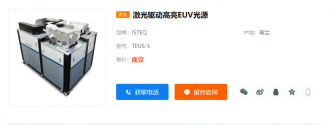
How the heck they generate EUV with this little setup? It doesn't have the room sized high power laser to zap the droplet.
I think they talk about the control and regulate the already generated EUV among the others rather than generation. But where they got their EUV from?

It has long been possible to generate small amounts of EUV in a lab setting with existing industrial lab equipment and processes - brief millisecond pulses at sub-watt power levels for materials testing and physics. But this is far from what's needed for high volume commercial chip lithography which requires hundreds of watts of light output and EUV pulses occurring so quickly it appears continuous, not to mention all the ancillary systems like tin debris management and thermal expansion that isn't a problem in a lab setting.
 

tokenanalyst

Brigadier
Registered Member
How the heck they generate EUV with this little setup? It doesn't have the room sized high power laser to zap the droplet.
I think they talk about the control and regulate the already generated EUV among the others rather than generation. But where they got their EUV from?

on another news, first 5 months, IC export value is bigger than car or Smart phones.
I wonder whether samsung or hynix fabs in China are biggest producers and count as export from China?

In terms of exports, in the first five months, China exported 5.87 trillion yuan of mechanical and electrical products, up 7.9%, accounting for 59% of the total export value. Among them, automatic data processing equipment and its parts were 554.46 billion yuan, up 9.9%; integrated circuits were 444.73 billion yuan, up 25.5%; automobiles were 329.7 billion yuan, up 23.8%; mobile phones were 329.68 billion yuan, down 2.8%.


Please, Log in or Register to view URLs content!
1717786123009.png
Or LPP
1717786246261.png
What is interesting in this setting is that Tsinghua seem to be generating EUV power with lasers instead of plasma.

Making EUV light is not impossible, patterning with EUV is more challenging. Require are little more complicated apparatus than just a light source.

"The project research team of Changchun Institute of Optics, Fine Mechanics and Physics, led by Jin Chunshui, has been adhering to the spirit of unremitting scientific research, devoting themselves to research, and accumulating experience. After eight years of hard work, they have made breakthroughs in core unit technologies such as ultra-high precision aspheric processing and detection, extreme ultraviolet multilayer films, and projection objective system integration testing that have restricted the development of extreme ultraviolet lithography in China. They have successfully developed a two-mirror EUV lithography objective system with a wave aberration better than 0.75 nm RMS, constructed an EUV lithography exposure device, and obtained the first photoresist exposure pattern with a line width of 32 nm for EUV projection lithography in China.

  Jin Chunshui said: "We have established a relatively complete exposure optical system key technology research and development platform, successfully completed the research content and task objectives deployed by the national major project, achieved a leap in EUV optical imaging technology, and significantly improved the core optical technology level of extreme ultraviolet lithography in my country."

  At the same time, the implementation of the project has formed a stable research team, laying a solid technical and talent foundation for my country to achieve sustainable development in the field of next-generation lithography technology.

  At the acceptance meeting, Jia Ping, director of the Changchun Institute of Optics, Fine Mechanics and Physics, pointed out that the EUV project is in a window period in terms of timing and technical difficulty, and hoped that the country would provide continuous and stable support. He encouraged the project participants to further leverage the advantages of EUV disciplines, work together with courage, and achieve better results with follow-up support."​
 

tokenanalyst

Brigadier
Registered Member

Ruilian New Materials plans to increase investment in optoelectronics by RMB 76.3984 million to strengthen its layout in the field of OLED materials​

Ruilian New Materials issued an announcement stating that the company and Idemitsu Electronics' shareholders Idemitsu Japan and Idemitsu (Shanghai) Investment Co., Ltd. (hereinafter referred to as "Idemitsu Shanghai") recently signed a "Joint Venture Agreement". The company plans to use its own funds to increase its capital in Idemitsu Electronics by RMB 76.398425 million in cash. After the capital increase is completed, the company will hold 20% of the equity of Idemitsu Electronics.

Idemitsu Kosan Co., Ltd. (hereinafter referred to as "Idemitsu Japan") is a major global manufacturer of OLED terminal materials. Its OLED luminescent materials rank first in the global market share and enjoy a high reputation in the field of OLED terminal materials. At present, the company's main products in the field of OLED materials are OLED pre-sublimation materials, and the company is a strategic supplier of OLED pre-sublimation materials for Idemitsu Japan.

As Idemitsu Japan intends to transfer most of its OLED material business in China to Idemitsu Electronics, the company will work with Idemitsu Japan to assist the joint venture in establishing an independent R&D and sales system. In order to actively respond to the localization demand for OLED materials, based on the company's strategic development and industrial layout needs, the company plans to make an equity investment in Idemitsu Electronics.

Please, Log in or Register to view URLs content!
 

tokenanalyst

Brigadier
Registered Member

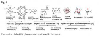
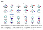
Accurate and efficient evaluation of the ionization potentials of extreme ultraviolet photoresists using density functionals and semi-empirical methods.​


School of Microelectronics, Shanghai University, Shanghai, 201800, China

Abstract​

Extreme ultraviolet (EUV) photoresists have become the core materials in lithography with nanometer-sized patterns and are actively explored on the path to realizing smaller critical dimensions. These photoresists can be small molecule-, polymer-, or organic–inorganic hybrid-based, with the full molecular working mechanism under investigation. For the rational design of EUV photoresists, theoretical guidance using tools like first-principle calculations and multi-scale simulations can be of great help. Considering the extremely high standard of accuracy in EUV lithography, it is critical to ensure the adoption of the appropriate methodologies in the theoretical evaluation of EUV photoresists. However, it is known that density functionals and semi-empirical methods differ in accuracy and efficiency, without a universal rule across materials. This poses a challenge in developing a reliable theoretical framework for calculating EUV photoresists. Here, we present a benchmark investigation of density functionals and semi-empirical methods on the three main types of EUV photoresists, focusing on the ionization potential, a key parameter in their microscopic molecular reactions. The vertical detachment energies (VDE) and adiabatic detachment energies (ADE) were calculated using 12 functionals, including pure functionals, hybrid functionals, Minnesota functionals, and the recently developed optimally tuned range-separated (OTRS) functionals. Several efficient semi-empirical methods were also chosen, including AM1, PM6, PM7, and GFN1-xTB in the extended tight-binding theoretical framework. These results guide the accurate and efficient calculation of EUV photoresists and are valuable for the development of multi-scale lithography protocols.

1717789080999.png
1717789109677.png

Please, Log in or Register to view URLs content!
 

tokenanalyst

Brigadier
Registered Member

Xinda Semiconductor signed a contract to achieve a "zero breakthrough" in domestic equipment!​


The SISPARK (Suzhou International Science and Technology Park) project - Xinda Semiconductor Equipment (Suzhou) Co., Ltd. (hereinafter referred to as "Xinda Semiconductor") signed a cooperation agreement with Jilin Qiushi Spectral Data Technology Co., Ltd. After the two parties reached a cooperation on the supply chain relationship, domestic front-end coating and development equipment will enter the OCF international supply chain for the first time, marking the localization of visualization chip color photoresist coating process equipment to achieve a "zero breakthrough", further accelerating the localization of key semiconductor core equipment, and promoting the high-quality development of the park's integrated circuit industry.

Xinda Semiconductor is a leading domestic semiconductor equipment manufacturer. It settled in the park in 2021 and is committed to the research and development and manufacturing of semiconductor front-end process - coating and development equipment. Its main products are coating and development machines (track) for semiconductor lithography processes.

The core R&D team of Xinda Semiconductor has more than 20 years of professional experience and has built a 3,500 square meter R&D and production site. The company uses Semi standard scheduling platform software and control system technology to realize the scheduling control of high-end coating and developing machine architecture and component modules, and uses the architecture platform technology of high-precision and high-capacity lithography products to realize the production and environmental control of stacked module architecture equipment. At present, the products have been completely localized from the overall architecture of the coating and developing machine to the unit components, which can replace imported products with lithography processes above 28nm from abroad, and can provide a series of services from complete machines to process solutions.

The company plans to complete the research and development, production, testing and sales of 14-28nm equipment in the next three years, consolidate the technology and market layout of front-end high-end FAB coating and developing machines, and it is expected that the total R&D investment in five years will exceed 100 million yuan.


1717789626997.png

Please, Log in or Register to view URLs content!
 

tokenanalyst

Brigadier
Registered Member
Beijing E-Town backed? Yita Semiconductor is covering all aspect of Rapid Thermal Processing in China, I think in a first.

Yita Semiconductor completed tens of millions of yuan in Pre-A round of financing​


Recently, Yita Semiconductor (Anhui) Co., Ltd. completed a Pre-A round of financing of tens of millions of yuan. The investors are Hefei Haiheng Science and Technology Investment Fund and related industry investors. This round of financing funds will mainly be used for the research and development, production, manufacturing and sales of MOCVD epitaxial systems and RTP rapid thermal processing system equipment.

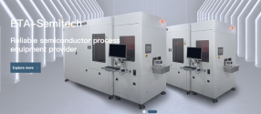
It is reported that ETA-Semitech is committed to the research and development of semiconductor process equipment and has successfully developed epitaxial systems (MOCVD) and annealing systems (laser annealing/RTP). The company has a number of technical solutions, including independent innovative SiC/GaN epitaxial growth solutions, rapid thermal processing (RTA), rapid thermal oxidation (RTO), rapid thermal nitridation (RTN), ion implantation annealing?, metal alloys, power chip back laser annealing and other solutions, and holds a number of patents and software copyrights.

ETA-Semitech was registered in February 2024, located in Hefei Economic Development Zone and is about to be put into trial operation. The total investment of the project is 350 million. The first phase of the project has a construction area of 4,000 square meters, mainly used for the research and development and production of MOCVD epitaxial systems and RTP rapid thermal processing systems. After the trial operation, the assembly and commissioning of the equipment will be officially started.

At present, Yita Semiconductor has two major production and research bases, located in Hefei Economic and Technological Development Zone and Deqing Zhejiang University of Technology Science Park (Yaoguang Semiconductor (Zhejiang) Co., Ltd.). After the completion of this round of financing, the development process of Yita Semiconductor's MOCVD, RTP and other equipment will be further accelerated.

1717790020912.png

Please, Log in or Register to view URLs content!


tokenanalyst

Brigadier
Registered Member

Annual production of 3,000 tons of high-purity quartz products! This project in Henan is under construction​

Ancai semiconductor [Introduction] Recently, the kiln heating ceremony of Henan Ancai Semiconductor's "Annual Production of 3,000 Tons of High-Purity Quartz Products for Photovoltaic and Semiconductor Use" was grandly held in the Science and Technology Incubation Park of Jiaozuo Economic and Technological Development Zone, Zhongzhan District, Jiaozuo City. China Powder Network News : Recently, the kiln heating ceremony of Henan Ancai Semiconductor's "Annual Production of 3,000 Tons of High-Purity Quartz Products for Photovoltaic and Semiconductor Use" project was grandly held in the Science and Technology Incubation Park of Jiaozuo Economic and Technological Development Zone, Zhongzhan District, Jiaozuo City.

Xu Dongwei, general manager of Henan Science and Technology Investment Co., Ltd. and chairman of Henan Huirong Asset Management Co., Ltd., attended the ceremony and said that at present, my country's semiconductor and photovoltaic application market has huge potential. He hopes that Ancai Hi-Tech will conduct extensive market research, effectively grasp market opportunities, extend and strengthen the chain around the leading industries, and strive to complete construction, put into production and achieve results as soon as possible. It is understood that Henan Ancai Semiconductor Co., Ltd.'s annual production of 3,000 tons of high-purity quartz products for photovoltaics and semiconductors is a key material for the new energy photovoltaic and semiconductor industries, and is used in the manufacturing of photovoltaic crystalline silicon cells and the semiconductor field. The total investment in the project is 199.15 million yuan. Ancai Hi-Tech said that high-purity quartz products are an indispensable and important basic material in the fields of photovoltaics and semiconductors. Their unique properties and wide range of applications give them broad market prospects. The quartz glass project is in line with the company's development goals and directions, and can promote the company's industrial upgrading and promote the company's high-quality development.​


Please, Log in or Register to view URLs content!
 

valysre

Junior Member
Registered Member
I have a few questions about the Chinese semiconductor industry, if anyone is interested in answering.
1) It seems that sub 14nm chips have been talked about a great deal regarding the Chinese semiconductor industry. Are there any real defense applications of such technology?
2) What are the motivations of the US to prevent China from producing sub 14nm chips? From a layman's view it seems that all the US has done is cut off its own access to a sizable market.
 

tokenanalyst

Brigadier
Registered Member
1) It seems that sub 14nm chips have been talked about a great deal regarding the Chinese semiconductor industry. Are there any real defense applications of such technology?
Are saying if is enough for military applications or if is more than enough for military applications?
If you are saying that if is enough for military applications let remind ourselves that:

This is the F-35 "SuperComputer"
1717798542077.png
As far I understand this is made in a 90nm CMOS planar process. In theory SMEE SSX-600 ArF machine can pattern this processors without not too much problem in a 300mm wafer. Even using the specs from 2011 that will give at least 50 wafers/hour that is absolutely more than enough for military production. That is not counting with the capabilities of making GaN and SiC and other high performance compound semiconductors ICs that will increase the military electronics performance of many weapons way beyond Silicon.

Please, Log in or Register to view URLs content!
2) What are the motivations of the US to prevent China from producing sub 14nm chips? From a layman's view it seems that all the US has done is cut off its own access to a sizable market.
Dysfunctional US Politics, Sheer stupidity and bunch of self appointed "industrial experts" that only care about their shallow agendas and no the industry destruction or the job losses that their recommended policies could create.
 
Top